Stabilizer Design Part 1
 Peter Polycarp
Electricity is the bedrock of contemporary society. It is deeply intertwined, and essential to the achievement of pertinent objectives in contemporary society.
Electricity supply in Nigeria is not only poor, when available; it is unstable (subject to heavy fluctuations). This instability has a disastrous effect on fragile (sensitive) and expensive electrical load. Nigerians have adopted several ways to acclimatize to this menace.
An automatic voltage stabilizer is an electronic device used to stabilize or regulate voltage within a certain voltage range. It can solve the problem right? Why not buy one?
MY MOTIVATION
I spent the second half of my 2021 in Ogwashi Uku, Delta state. During my stay there, I experienced what I prefer to call virtual electricity — low voltage supply there could be electricity for 24 hours, albeit, absolutely useless.
This period of virtual electricity meant I was unable to work on any project (my boss didn’t own a generator), which was very frustrating.
In light of the aforementioned events, my boss borrowed a 1KVA automatic voltage regulator. I was asked to use it for soldering components to a PCB (Printed Circuit Board) and trouble shooting.Unfortunately, the transformer coil got damaged. This is probably due to short circuit or overload. Exempting, the input voltage protection via fuse, the regulator had neither short circuit nor overload protection capabilities.
This culmination of unplanned incidents, and my drive for personal development, prompted my interest in developing an automatic voltage stabilizer.
Join me as we drive into my world of "desolerny" aha! 😉😉 — I guess you don't know what it means. Well, it is my own word for: learning to design; designing to learn (design of learning).
SPECIFICATIONS AND FEATURES
The automatic voltage stabilizer will be designed to encompass these essential features:
- Constant frequency ( input frequency is same as output frequency)
- Output Voltage within 215V- 240V
- High cut off feature
- Low cut off feature
- No microcontroller ( to improve on my ability to work with discrete analog and digital ICs).
- Short circuit detection and protection
- Overload detection and protection. Therefore, the system design will be optimized to satisfy the following standards:
- Input voltage range: 140V - 290V
- Output voltage range: 215V - 240V
- Power rating: 1KVA ( adjustable)
- high cut off voltage: 290V
- Low cut off voltage: 140V
Stabilizer Design
The stabilizer design will be categorized into:
- Control Stage design
- Power stage design
CONTROL STAGE DESIGN
The control stage, as it name implies, will be designed to control the power stage. Therefore, it will constitute of:
- Input voltage detection circuit
- Protection circuits
- Indicator and display circuits
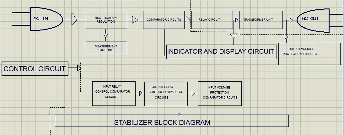
Input Voltage Detection Circuit — Design, Rationale and Conclusions
The input voltage is from the national grid. Detecting its presence and magnitude is essential to the efficacy of my design.
To that end, the input voltage detection stage/circuit will comprise of:
- Rectification, regulation and filtering circuit
- Sampling and measurement circuit?
- Schmitt trigger/comparator circuit:
- Input voltage relay control
- Output voltage relay control
RECTIFICATION AND REGULATION
An auxiliary winding from the power transformer in the power stage is used to power the circuit. The output of the auxiliary winding is rectified via a simple bridge rectifier and filtered with a bulk and decoupling capacitor. Linear regulator (LM317T) will be used to regulate the output of the rectifier. This regulated voltage is used to provide reference voltage in the Schmitt trigger design. The output of the linear regulator is also used to power the relays in the power stage.
Furthermore, the input voltage (from the grid) is rectified, filtered and stepped down with the aid of voltage divider circuit. The output of the voltage divider circuit is applied to the input terminal of the Schmitt trigger.
A clamp circuit comprising of two diodes is used to protect the ICs in the event of an overvoltage or under voltage (relative to the maximum input voltage of the comparator ICs) at the voltage divider output. Fluctuations maybe caused by changes in tolerance of the resistors.
SAMPLING AND MEASUREMENT
One of the many rationales behind this project is to test the limit of my ability to construct circuits without a microcontroller. The ADC and interrupt routine of an 8 bit microcontroller will suffice for sampling and measurement.
Nevertheless, without a microcontroller, I got my voltage sampling by using simple ratio and proportion.
$$ \dfrac{a}{b} = \dfrac{d}{c} $$
Similarly, I used 290V as my maximum AC input, and 12V as my maximum DC output from the voltage divider. Rectified AC at 290V equals approximately 410V — (peak voltage i.e. $$290 \times \sqrt{2}$$ ) Therefore the AC voltage to DC voltage rating is given by:
$$ \dfrac{410}{12} = \dfrac{x}{1} $$ Where X equals: peak AC voltage when DC voltage equals 1. Using this logic, I arrived at voltage sample of: $$34.1 :1$$. In other words rectified DC Voltage = $$\dfrac{AC voltage \times \sqrt{2}}{34.1}$$
AC voltage Vrms = $$( (DC voltage \times 34.1) \times 0.7071))$$ The rectified and sampled input voltage is connected to the input pin of the Schmitt trigger.
SCHMITT TRIGGER CIRCUIT
Input relay comparator control
The input relay comparator is designed to control relays connected to an autotransformer.
The comparators are configured in the non-inverting topology. Each comparator measures a voltage range within 140V - 290V range. Thus, the 140V - 290V range is sub divided into:
- 140 – 165
- 166 – 190
- 190 – 240
- 240 – 265
- 265 - 290
This subdivision entails the use of 5 comparators with hysteresis
Furthermore, the comparators are used to drive transistor switch in the simple common emitted configuration. Similarly, the transistors are used to drive relays.

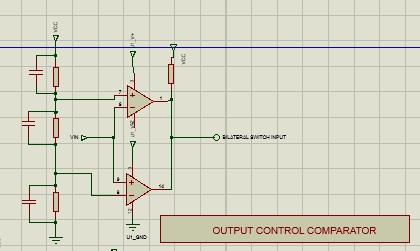
Output relay control comparator
The output comparator relay drivers are designed to detect voltage level at a certain range and switch between 215V and 240V tapping of the auto transformer.
The output comparator relay driver is based on a random guess work I intend to put to test.
This stage is achieved with the aid of a window comparator. Each of the voltage range in the input control stage will further be divided into high out (240V) and low out (215V) tapping of the autotransformer.
For instance, the 140 - 165V range is subdivided into:
| Voltage Range | Output tapping |
| (140V – 156V) — High out | 215V |
| (157V – 174V) — Low out | 215V |
This design is done for each voltage range. The output for each voltage range is connected to a bilateral switch configured as a de - multiplexer. Thereafter, the output of the bilateral switch is used to drive the relay via a transistor
PROTECTION CIRCUITS
Any power electronics device without adequate for its internal circuitry or electrical load isn't far from useless. Exempting quality of components used, the durability of a power electronic device depends on the potency of its protective circuit. Thus, this stabilizer design incorporates overload and short circuit protection.
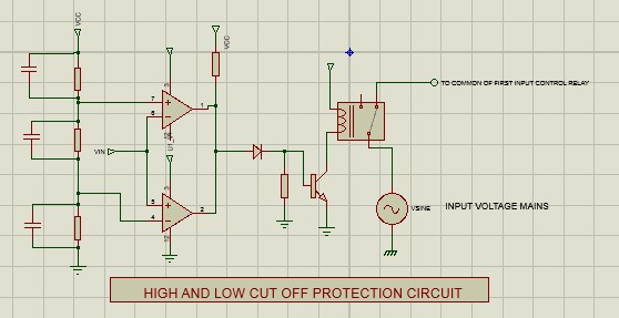
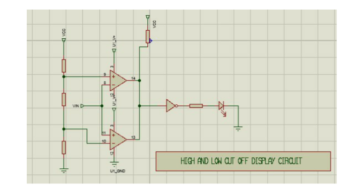
Furthermore, the high and low cut off feature are implemented with the aid of a window comparator. The window area of the comparator encompasses the feasible voltage range of the stabilizer.
OVERLOAD PROTECTION CIRCUIT
To design the overload protection circuit, I figured overload is associated with over current and reduction in voltage.
Given a 1 KVA stabilizer:
$$
P = VI,
\quad I = \dfrac{P}{V}
\quad V = \dfrac{P}{I}
$$
Assuming PF = 1
Maximum output current $$I =
\dfrac{1000}{240} \approx 4.2A$$
Where: P = Power, V = Voltage, and I = Current
Given the above equations, it is deducible that there is an inverse relationship between current and voltage provided power is constant.
Furthermore, the current is converted to voltage using ohms law.
V = IR
To that end, the overload protection circuit incorporates a current sense resistor, differential amplifier and comparator configured as a Schmitt trigger in the non - inverting mode. The voltage across the current sense resistor is compared with the maximum allowable current, that has been converted to voltage via the current sense resistor.
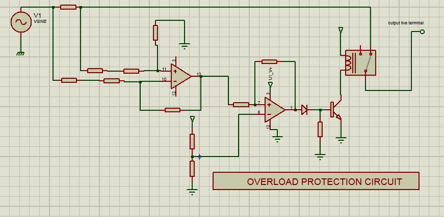
I know! I know! Appling 240VAC to the input of an OPAMP is stupid. What about common mode voltage! It won’t work in the linear region!
Well, the resistors will be of high value, and I may add DC offset to the circuit. Summarily, this circuit will undergo slight changes. For instance, I may ditch discrete OPAMP (Operational Amplifier) for high common mode voltage difference amplifier like AD629 (± 270V) or INA149 (± 275V). However, this is the basic idea behind the circuit design. I know you are thinking of CMRR (Common Mode Rejection Ratio), right? Don’t worry.
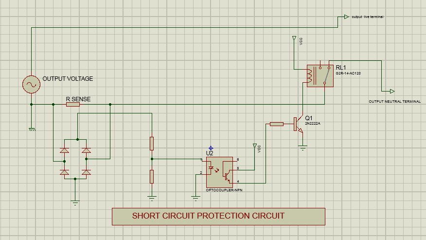
SHORT CIRCUIT PROTECTION
In a DC circuit, during short circuit, the current increases to near infinity; voltage reduces to a negligible value (considered zero volts).Therefore continual measurement of battery voltage in the event of sudden voltage drop can be used to detect short circuit.
However, in an AC circuit, I didn't know how to go about it. Even if I know that, when there is a short between the live and neutral wires, there will be zero potential difference between both wires, howbeit, the maximum voltage in the circuit relative to ground will be 240V (depending on location).
I also know that the voltage at the neutral wire should be zero volts at all times. Utilizing this knowledge, I placed a resistor in the neutral wire. When there is a short circuit, the voltage across the resistor will be rectified, and stepped down with a voltage divider. The output of the voltage divider is then connected to an optocoupler, which is in turn used to drive a relay via a transistor switch.
LED INDICATOR AND DISPLAY CIRCUIT
This should be the easiest part of the control designing monologue — yeah! I have just been thinking. Part II will prove my hypothesis to be either correct or flawed
The indicator circuit is more like a GUI (Graphical User Interface). This circuit will help the user interact (maybe that's not the word) with the stabilizer without much ado.
This circuit will be based on LED indicators and buzzers to show:
- Low and high input cut off mode
- Short circuit protection mode
- Overload protection mode
The high and low input indicator circuit is based on a window comparator. The window area of the comparator encompasses the whole operating range of the stabilizer.
The output of the window comparator will be connected to NOT gate. This NOT gate is used to invert the output of the comparator. The output of the NOT gate is then used to drive a relay via a transistor switch.
My initial intent for displaying the output voltage is to connect an analog voltmeter to the output terminals. However, I have decided to try interfacing a seven segment LED to the circuit with no microcontroller. Therefore, it’s either a seven segment led, if successful, or an analog voltmeter.
The display circuits for overload and short circuit are similar to the ones I explained before.
POWER STAGE
The power stage is probably the easiest of my design. It's just like every other stabilizer, except, it will have too many relays. I am considering the option of using solid state relays (SSR). Schematic of the power stage will be discussed in part 2.
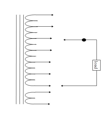
The power stage is simply a combination of relays connected to the input tappings of an autotransformer. An autotransformer? What's that? Here's the schematic symbol:
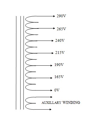
My autotransformer isn't complex, its turns ratio will probably be:
- 165:190:215:240:265:290 or
- 165:190:215:240:290
My auto transformer schematic:
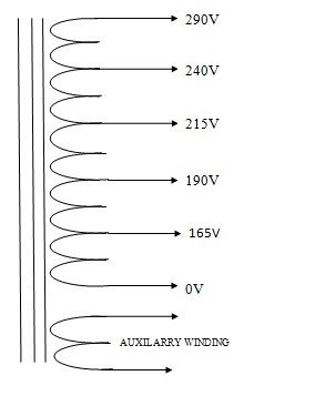
I won't treat transformer design procedures in the next part. That's a whole topic on its own. If you are a bit rusty I suggest you use:
- Transformer and Inductor Design Handbook — Colonel Wm. T. McLyman
- Practical Transformer Handbook — Irving Gotlieb
The wire gauge and values used for overload shutdown design will determine the output power. To that end, both the power stage and control stage will be on different boards. A preset/pot will be used in the overload comparator. This is to ensure the maximum output power can be adjusted.
End Note: I know the components used are much and unnecessary (given comtemporary technology). However, I just want to test my proficiency in analog electronics
Subscribe to my newsletter
Read articles from Peter Polycarp directly inside your inbox. Subscribe to the newsletter, and don't miss out.
Written by

Peter Polycarp
Peter Polycarp
“Design and implementation gives me purpose, documentation and teaching illuminates my path.” As a teenager, I developed an interest and enthusiasm for the decision-making capacity of electronic devices. This enthusiasm drives my passion for designing and implementing electronic systems with the ability to make smart decisions and interact with their surroundings. In a similar vein, taking note of each stage of project design and implementation provides me with an opportunity to share my experience and get feedback. This feedback illuminates the path for a new project. The design and implementation of embedded systems, together with documentation and explanation of the processes involved, can be considered as a learning element. I believe there is nothing better than learning and mastering new concepts. So, what's your next design idea? Do you need a Workshop Assistant for your embedded system design? Do you need help documenting or conducting research in your embedded systems design project? Get in touch with me right away at peterpolycarp25@gmail.com. You’ve got nothing to lose !!