Crafting Magical Memory: Building RAM from Mystical Bits
 Vinod Murugan

Have you ever wondered how your computer remembers all your stuff, even though it's just a machine? Today, we'll explore a vital part of this magic: RAM (Random Access Memory), this blog will help you build your own RAM from scratch and at the end you will be convinced that it is actually MAGIC.
Prerequisites : You should have a letter from Hogwarts School of Witchcraft and Wizardry(seriously) to learn this. (Please watch all the snippets attached with this blog so that you can visualize things better). Open this in new tab, it will help you view draws side by side and make it easy for you to follow:https://excalidraw.com/#json=QLMdBSAxySbT3luyhWPlq,enN9qT4Lv1_iZaHO8N-4Xw (Excali draw)
So let's start with what computers actually understands, think of a computer like a complex light bulb. A light bulb has two states: on (when current flows and it lights up) and off (when no current flows and it's dark). This is exactly what computer understands, it is a machine and it cannot understand actually I'm using it alot just so it gets to you, it's a machine that we can control by allowing current to pass or stop the flow basically in technical terms "they can process information based on the presence or absence of electrical signals". An "on" state, when electricity is flowing, represents 1. The "off" state, no electricity is flowing, represents 0.
Now let's know the core magical element that builds it all, that is TRANSISTORS. Transistors are semiconductors that is they can allow the current to flow or stop the current from flowing, Imagine it more like a water tap which when turned on let's the water through it.
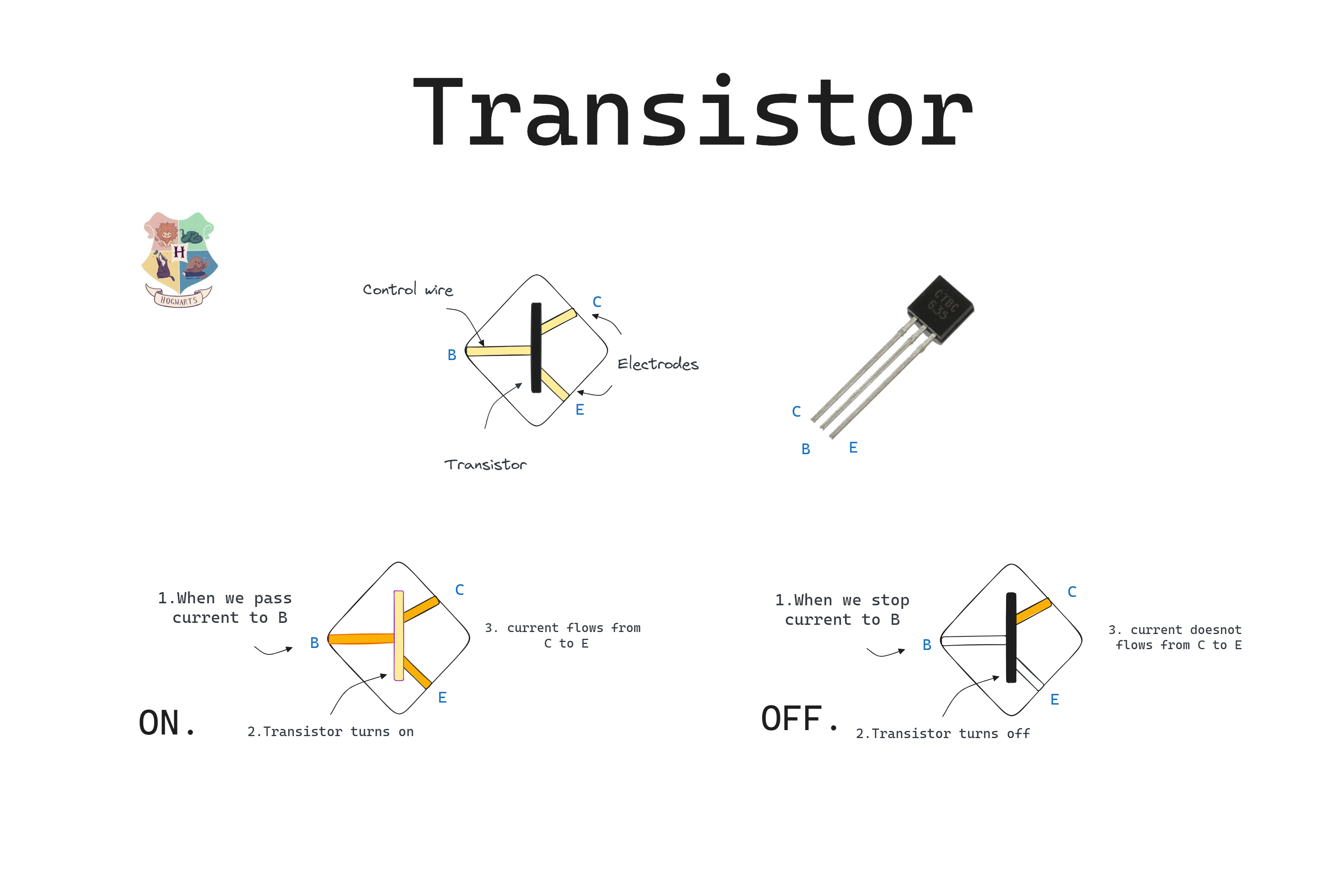
Now see the above diagram certified by Hogwarts, this is how a transistor looks, it has two electrodes and a control wire. When current flows through the control wire the transistor turns on and allows the current to flow from electrode C to electrode E, and if we don't pass current to the control wire, the current will not flow from electrode C to electrode E, more like a switch. Now we are able to control the flow of current by allowing it and stopping it from flowing in certain circuit.
From now on instead of current flows I will call it as 1 and current doesn't flows is 0. So above if input(control wire) is 1 then output(electrode E) is 1, if input is 0(control wire) then output is 0(electrode E).
We've explored how transistors act like tiny switches, controlling the flow of electricity (1) or stopping it (0). But how do we use these 0s and 1s to make actual decisions? Enter Boolean Algebra, the magical rulebook that governs the logic behind computer operations!
Think of it like a special math class for 0s and 1s only. Unlike regular math with numbers, Boolean Algebra deals with these two binary values and how to manipulate them. It's like a secret language computers use to make choices and perform calculations.
The Three Basic Spells:
Just like any good magic system, Boolean Algebra has its own set of spells (operations) to work with 0s and 1s. Here are the three most fundamental ones:
NOT: This spell is like a logical "flipper." It takes a single 0 or 1 as input and gives you the opposite as output. If your input is 1 (think "true"), NOT flips it to 0 ("false"). Conversely, if you input 0 ("false"), NOT changes it to 1 ("true").
AND: Imagine this as a two-person spell. It requires two inputs, both 0 or 1. The spell only casts successfully (outputting 1) if BOTH inputs are 1. Any other combination (0 and 0, 0 and 1, or 1 and 0) results in a failed spell (outputting 0). Think of it like needing two keys to unlock a magical door - both keys (both inputs being 1) are needed for success.
OR: This spell is a little more lenient. It also takes two inputs (0 or 1) and outputs 1 if EITHER input is 1. Only if BOTH inputs are 0 will the spell fail (outputting 0). Imagine this as opening a magical gate with two levers. Pulling either lever (one input being 1) is enough to open the gate.
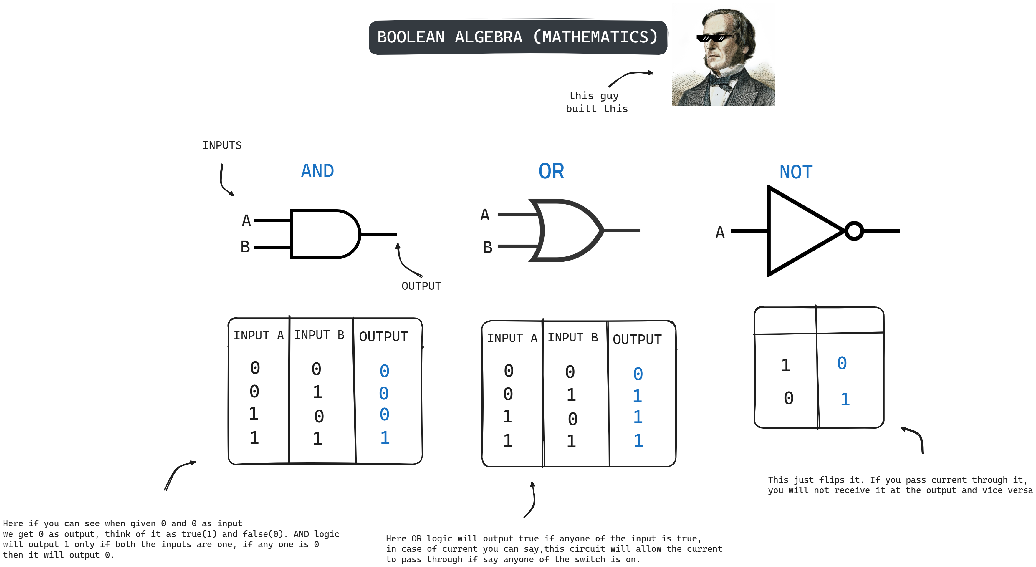
I understand you got to be saying we jumped from current, transistors to mathematics, I know you hate it but bear with me, you will understand why it is important and for what purpose it was used once you read this blog completely.
For now just treat this as a simple algebra section in which there are 3 operations and as you can above they have a nice little diagram to denote all three and a table below it. Some operation like AND, OR takes 2 inputs and outputs one value. These table denotes all the possible inputs that you can give and the outputs that you will get.
The most interesting part is that we can build these boolean logic out of transistors.
Let's build a NOT boolean logic using transistor in which if we pass 1 then we will get 0 and vice versa.
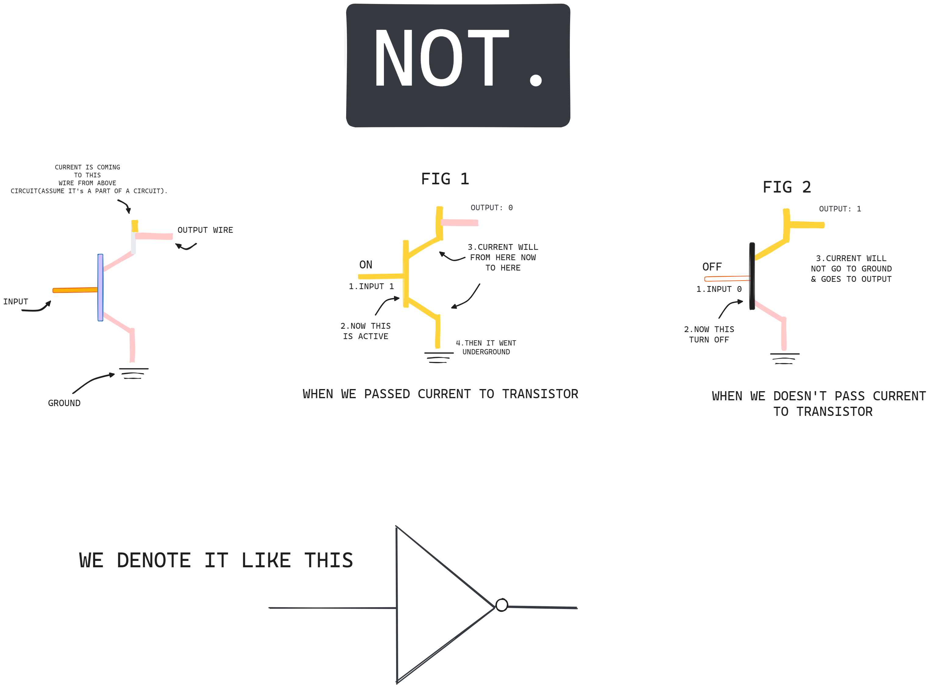
We can modify this circuit just a little bit to create a NOT. Instead of having the output wire at the end of the transistor, we can move it before. If we turn the input on(passing current to transistor), the transistor allows current(from above circuit or say a some wire) to pass through it to the “ground”, and the output wire won’t receive that current - so it will be off (FIG 1). In our water metaphor grounding would be like if all the water in your house was flowing out of a huge hose so there wasn’t any water pressure left for your shower. So in this case if the input is on, output is off. When we turn off the transistor(not passing current to transistor), though, current is prevented from flowing down it to the ground, so instead, current(that above circuit one) flows through the output wire(FIG 2). So the input will be off and the output will be on. And this matches our logic table for NOT, so congrats, we just built a circuit that computes NOT!
We call them NOT gates - we call them gates because they’re controlling the path of our current.
Congratulations, We just created our first NOT gate using transistors. We learned our first magic "Wingardium Leviosa".
Now similarly we can create AND and OR Gates.
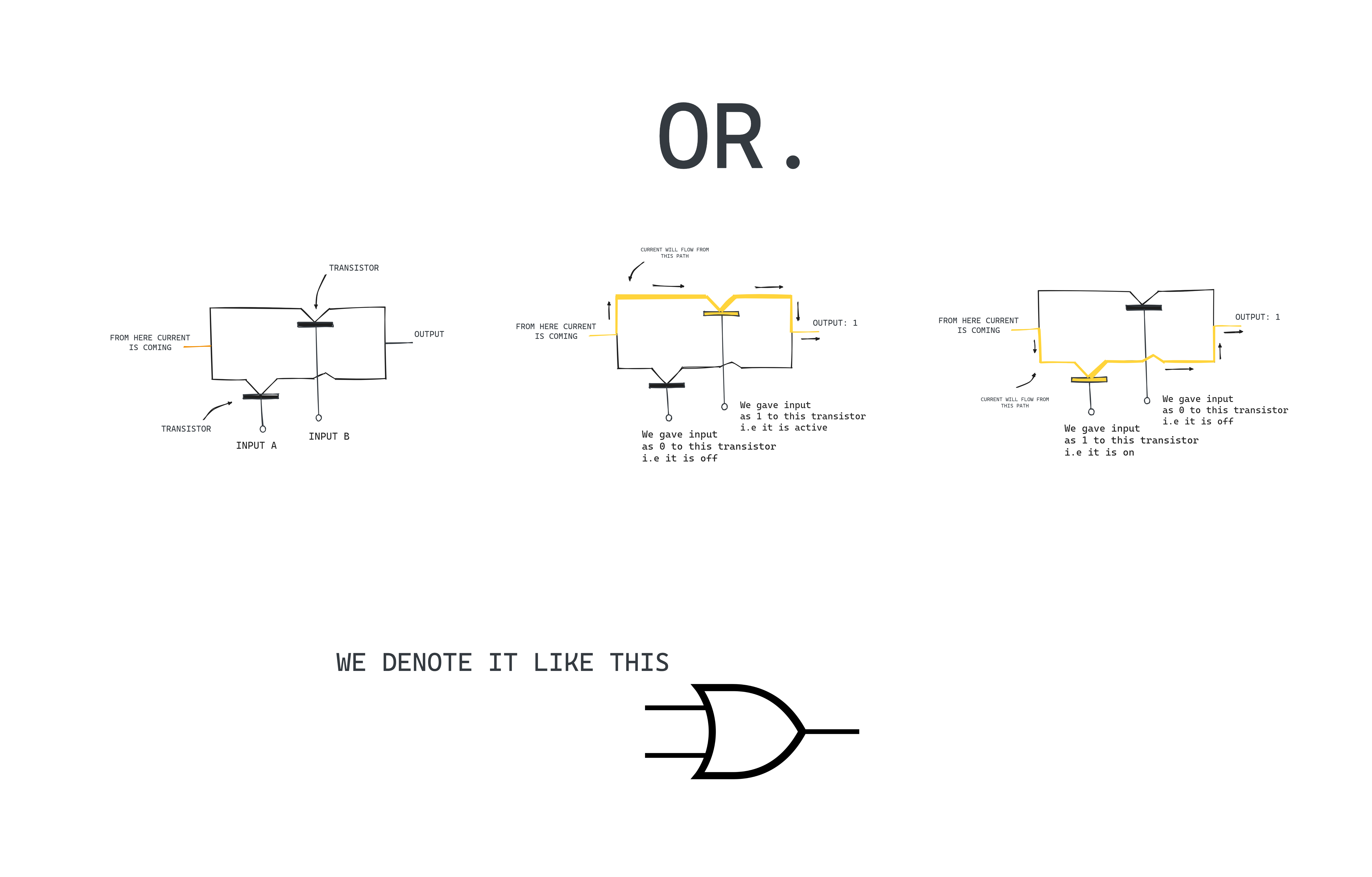
Here we built an OR gate, we have attached transistors in parallel. Imagine it as two paths for you(current) to take, if any one is active you will go through that and you can see that I have taken two cases, at first we passed 1 i.e current to upper transistor making it active and passing 0 to the below transistor so it will not let the current to pass through it, but the upper one does. Hence we got 1 i.e current at the end. In case 2, the inputs are just reversed. If we have given both inputs as 0 then the output will be 0 as none of them will let the current to pass through them.
Reiterating it again to avoid any confusions, we pass inputs 1 or 0 to transistors and based on it we get the output i.e 1(current) or 0(no current).
Let's build an AND Gate now.
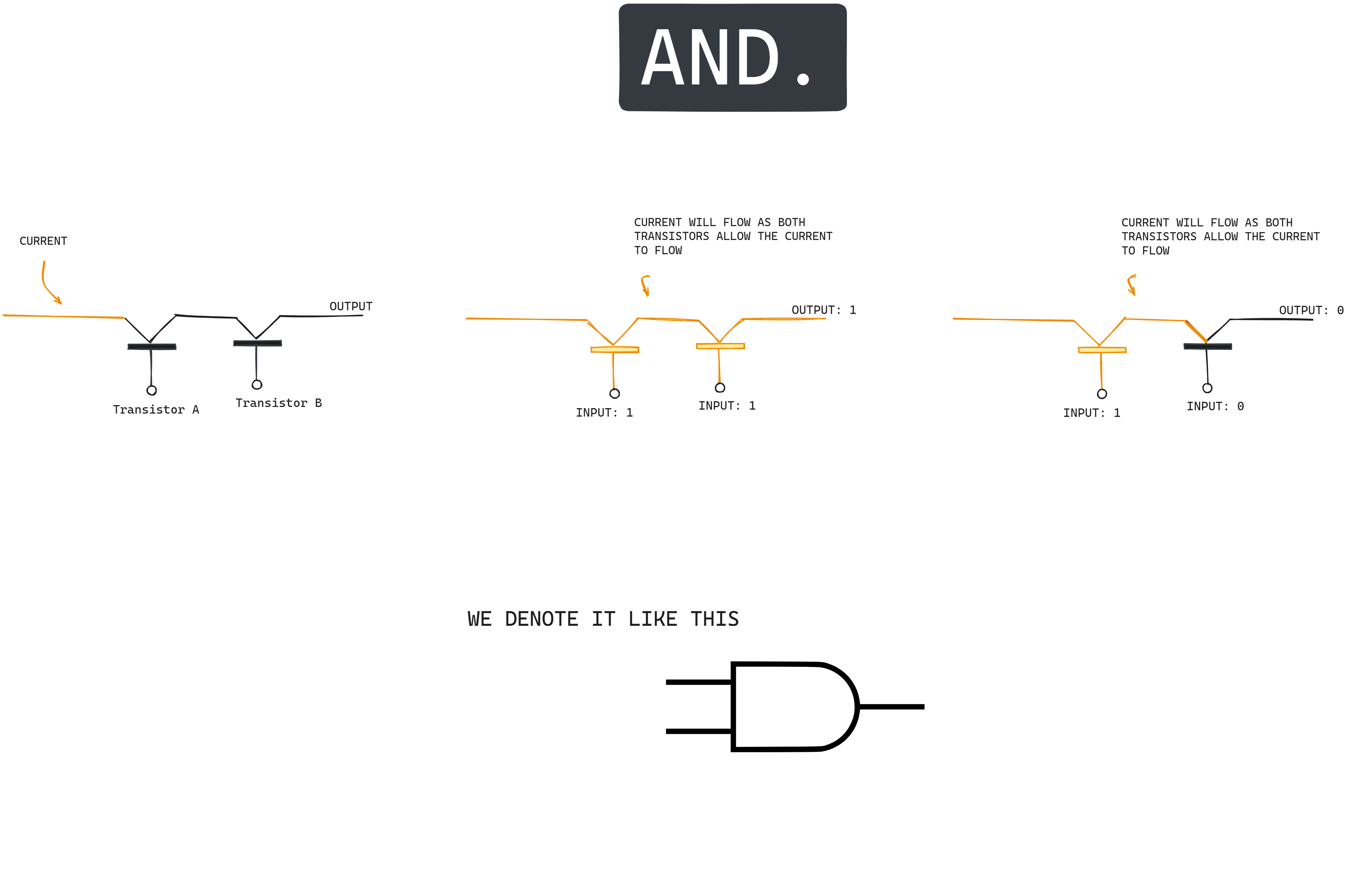
So here we have attached two transistors in a same path, so now both has to be turned on in order for the current to pass. So in first case(the middle diagram), we have given input as 1 and 1 and got output as 1. In second case(last diagram), we passed 1 and 0 and got 0 as one of the transistor(last one) didn't let the current to pass through it.
There are more like XOR, NOR and all these are built from the above three fundamental gates. You can look it up from internet**(not at all necessary for this blog)**.
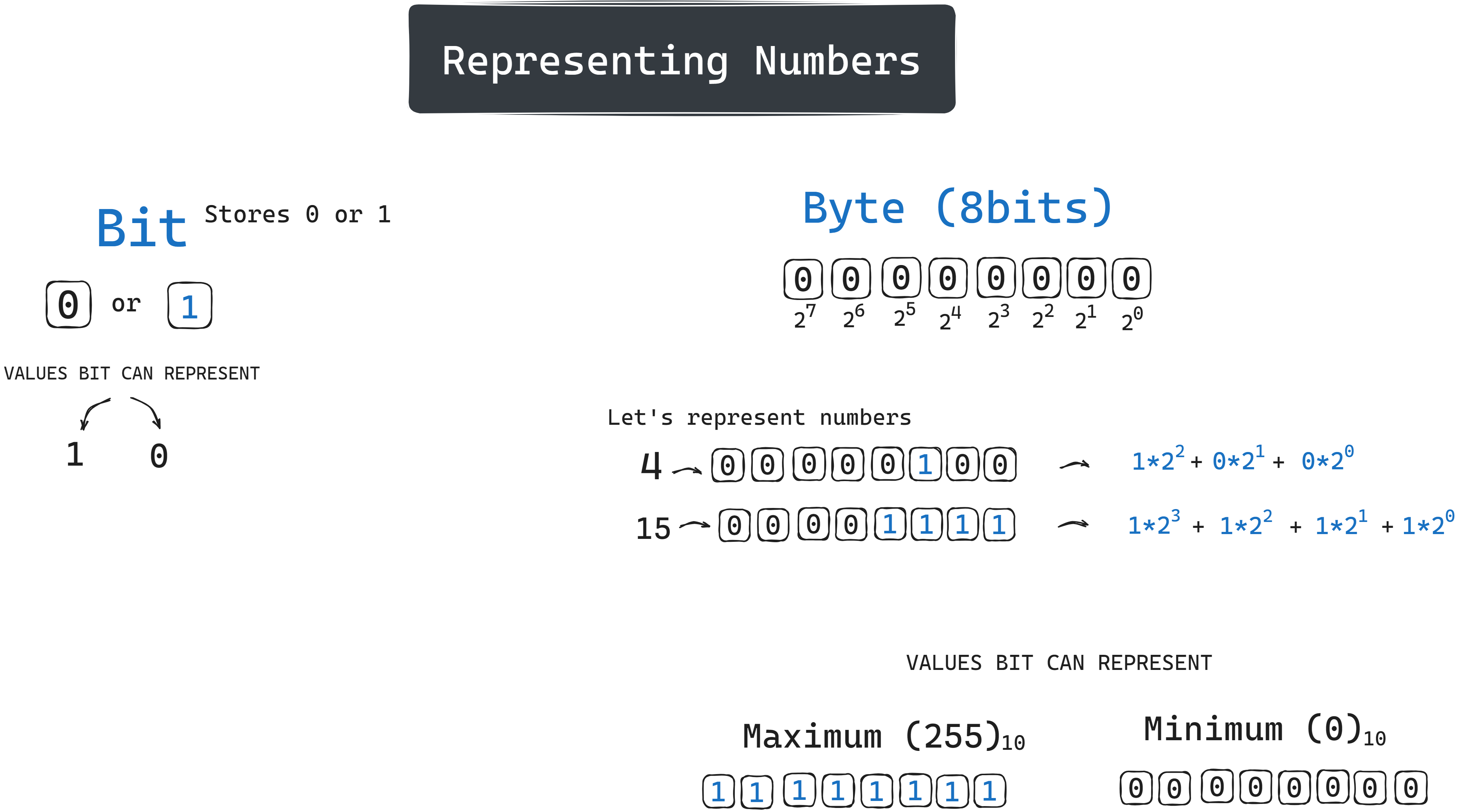
Ok so we are done with basics which tells you that your computer operates only and only in 1's and 0's. So now it is necessary for you to know how a computer represents a number in order for you to build a place for it to store. So it is simple, computer stores numbers in the form of 0's and 1's cause it doesnot understand anything else at all, even 0's and 1's are not number here these are states representing current. So say there is a little container that can store 0 or 1 that is maximum value it can represent is 1 and minimum value this container can represent is 0(in number), this is what we call as a BIT.
Let's take 8 of those containers and now these 8 container together can store a maximum value of 255(all container stores 1) and a minimum value of 0(all container stores 0). Look at the diagram representation I attached for you to get it even better.
Till now we have learned what are computers process, what are transistors, boolean algebra, how logic gates looks like and making our very own circuits from scratch. So now we are equipped with our wand and an owl, now it's time to get out of Diagon Alley and learn the magic.
Now we will bring this to life by our spell. We can create circuits that can loopback on itself, Like in OR and AND gate that we created we can feed the output of it to one of it's input. Seems amazing right. Let's see this in figure then I will explain.
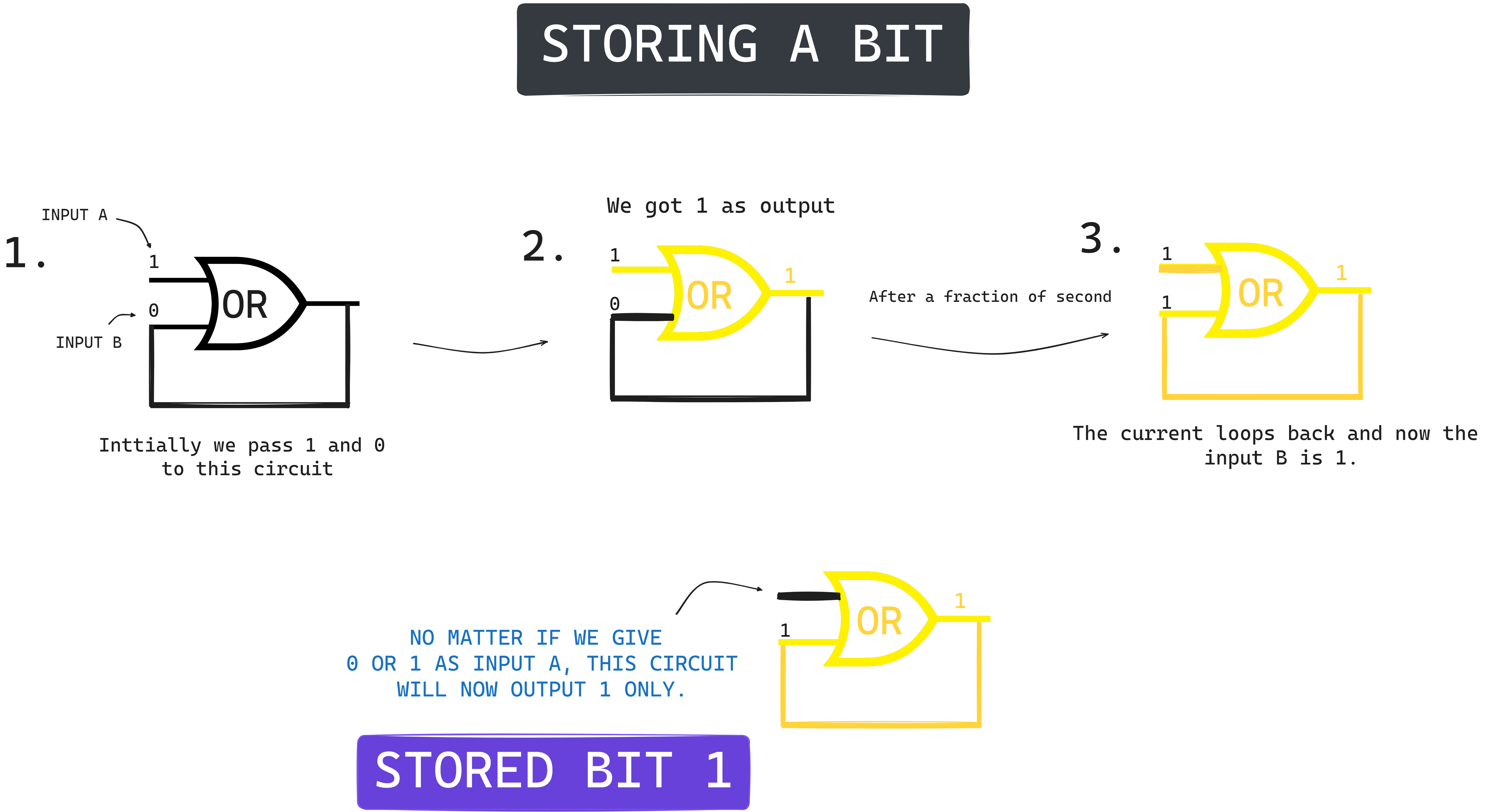
Here we initially set inputs as 1 and 0 and since we are using OR gate we got 1 as output. After a fraction of second this output that is 1 loopsback to input B and now the value of B is 1. So now no matter the input at A be it 0 or 1 this circuit will always output 1 cause the input B is untouched. Hence, you created your first ever memory which permanently stores 1.
Let's now create a circuit similar to this but it will store 0 permanently.
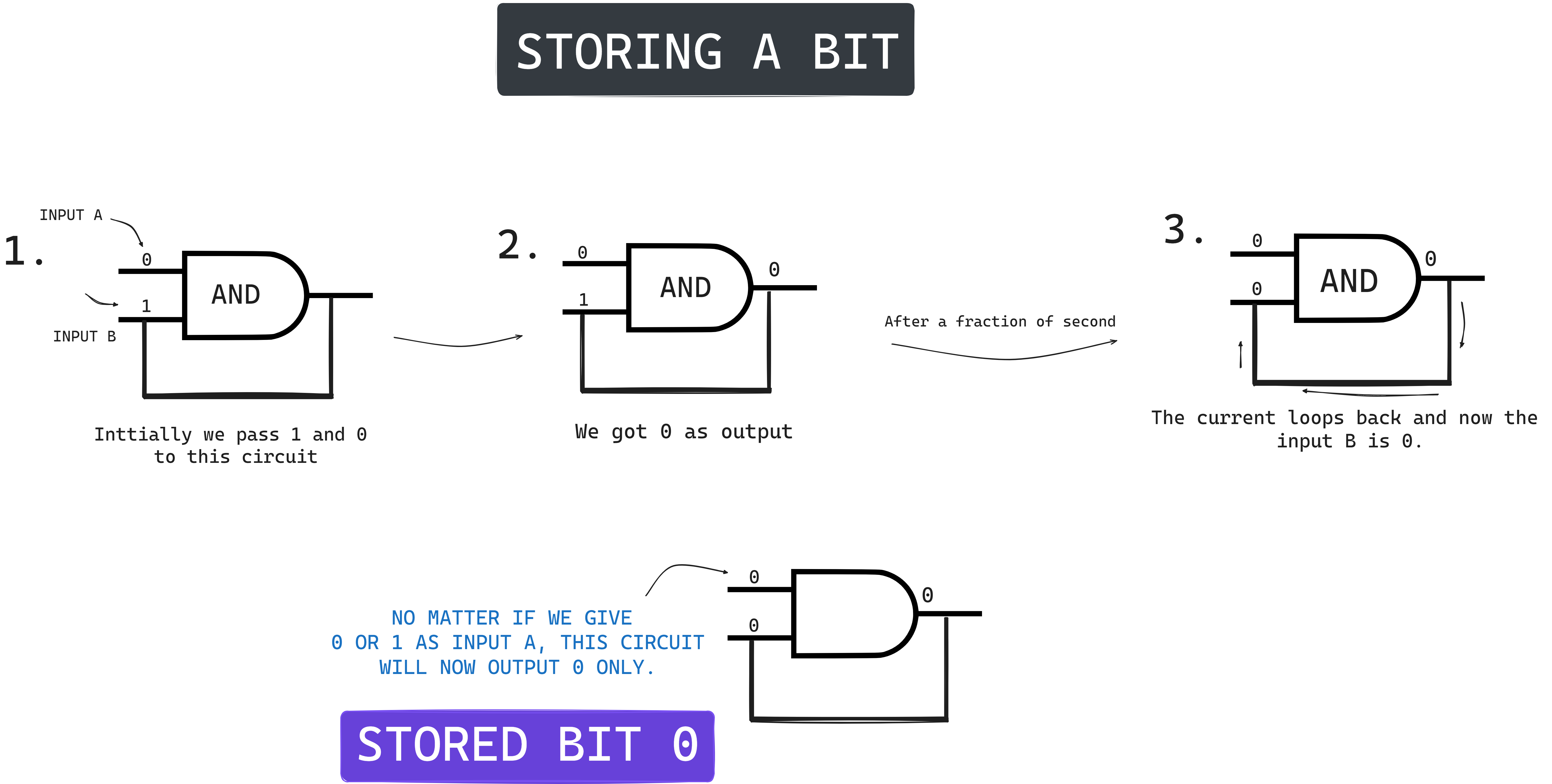
Here we took an AND gate, we set inputs to 0 and 1 at start, now since it's an AND gate we get the output 0, now after a fraction of seconds since we have a feedback loop here the input at B becomes zero and now no matter waht input A has 0 or 1, it will only result in 0, thus storing 0.
Now you have become a potion apprenticeship, but but but...
Why This Isn't Real RAM:
Real memory needs to be more reliable. It should remember the value we set (like "on" or "off") even if the original input changes. In simple terms, it should remember it's previous state and we should also be able to change it according to us.
This simple OR/AND gate loopback circuit doesn't meet that requirement.
Now let's create something that will meet these requirement. We got the purpose that we should have a single circuit that will be able to switch between states(0 and 1) and also should remember the previous state.
The key to making this a useful piece of circuit or say memory(we can say that now, Lumos!). Again we have to unravel the ancient scroll of deep magic which is called AND-OR Latch and it latches onto wizards to keep itself immortal.
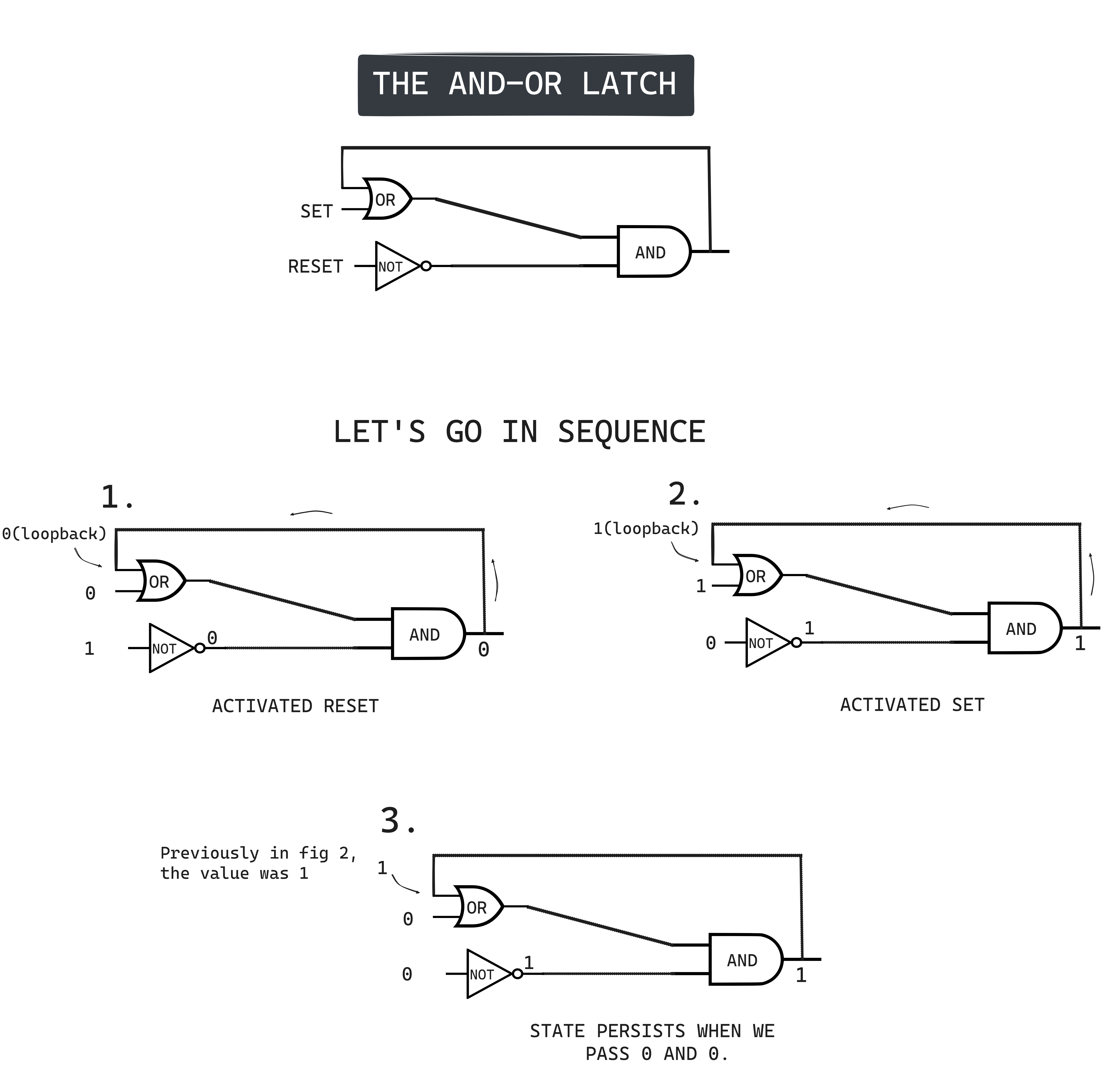
So here is your AND-OR Latch. In this there are 2 inputs SET and RESET. If RESET is 1 and SET is 0 then this latch will store 0 and if SET is 1 and RESET is 0 then this latch will store 1. If both the inputs are zero than it will persists it's previous value. Let me explain the above. In Step 1, we set SET as 0 and RESET as 1, then the result of OR is 1 and the result of NOT is 0, so at AND we got 2 inputs 0(from OR) and 1(from NOT) and this AND resulted in 0. After a fraction of second, this 0 loops back as an input to OR. So now this circuit will output 0.
Now see the next step 2, we wanted our latch to store 1, so we turned on SET and turned off RESET. So now in OR gate we have 2 inputs a 1 (that we set currently) and the previous loopback state it got that is 0(from fig 1). So this OR results in 1 and the NOT outputs 1 as it was given 0. The AND receives 2 inputs, 1(from OR) and 1(from NOT) and this AND will result in 1 and this 1 OR gets as one of it's input. So now this latch is storing 1.
Now the 2 figure shows that this latch will persist data that is it remembers it's last state it was in, so we passed 0 to SET and 0 to RESET. Now the OR gate has 2 inputs one is 0(that we just gave as input) and 1(from feedback loop from previous operation) and this OR gate outputs 1 and we passed 0 to NOT gate and we got 1 as output. Now these two will serve as inputs to AND gate and we will get 1 as output from AND gate, thus preserving the previous value.
This is called "LATCH" because it latches onto a particular value and stays that way. The action of putting data into memory is called "Writing" (this is what we did), whereas getting the data out is called "Reading".
But still having two inputs are confusing from a circuits point of few(even I got tired making these draws). So we upgraded. By using few extra logic gates we are able have just one input for SET and RESET both. Previously we had two one for 1(SET) and other for 0(RESET). Now it is possible with one and it's called "Gated Latch" and you can look it up how it is created but here I will use a simple illustration for it.
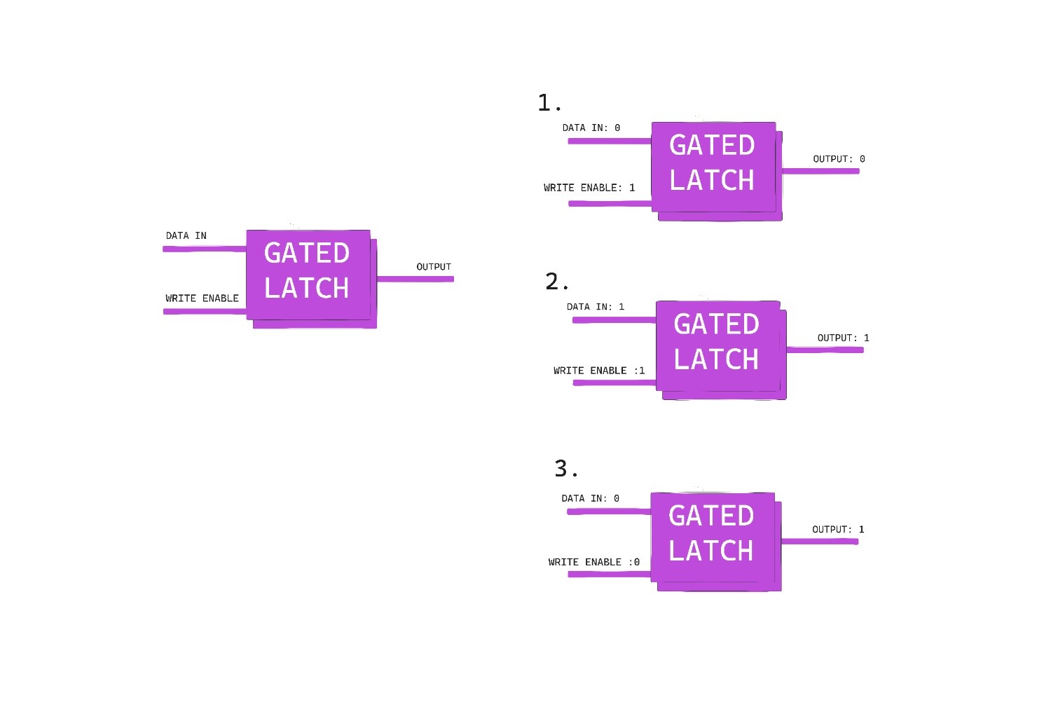
So here if write enable is 1 then only we will be able to set data in the latch and if write enabled is 0 then we can't change the data present inside the latch, it will stay as it was set previously. Acts like a gate, if gate is opened value can be changed and vice versa.
So we are successfull able to create our very own MEMORY and yes it is a memory of Dumbledore's past with Tom Riddle.
Since it stores only 1 bit that is either 0 or 1, we should have more that one in order for us to store more information like 8 bit numbers (refer the "REPRESENTING NUMBERS" draw that I have attached above). So we lined 8 of this gated latch in order to store 8 bit numbers.
A group of latches operating like this is called a register, which holds a single number, and the number of bits in a register is called its width.

In this we took 8 gated latches, and each latch has a data input wire denoted using "D" through this we will give our input, data out is where the data stored inside the latch is represented and a write enable wire that we just studied above like if it's active we can write data else no. So we have 8 latches and 16 wires(data in and data out) + write enable wire at the bottom which is common for all cause we can have just one write enable wire which can signal latches that if we can write or not. So if this write enable wire is 1 then we write 10110101 by giving each bit to corresponding latches.
Now since we can store 8 bit numbers by having 8 latches let's store more data so what we can do is say for 64 bits data let's take 64 latches and align them together but the issue will be for 64 latches 128 wires will be required. 1 latch takes two wires one for input and other for output plus one for write enable wire so in total 129. So we can still do it but we have Hermione, she suggested something let's look at it.
Hermione suggested instead of aligning the latches in a row, make use of grid/matrix. So let's create 64 bits memory by placing latches in 8 x 8 matrix. Let's unravel one more cursed scroll that opens up a portal to new world.
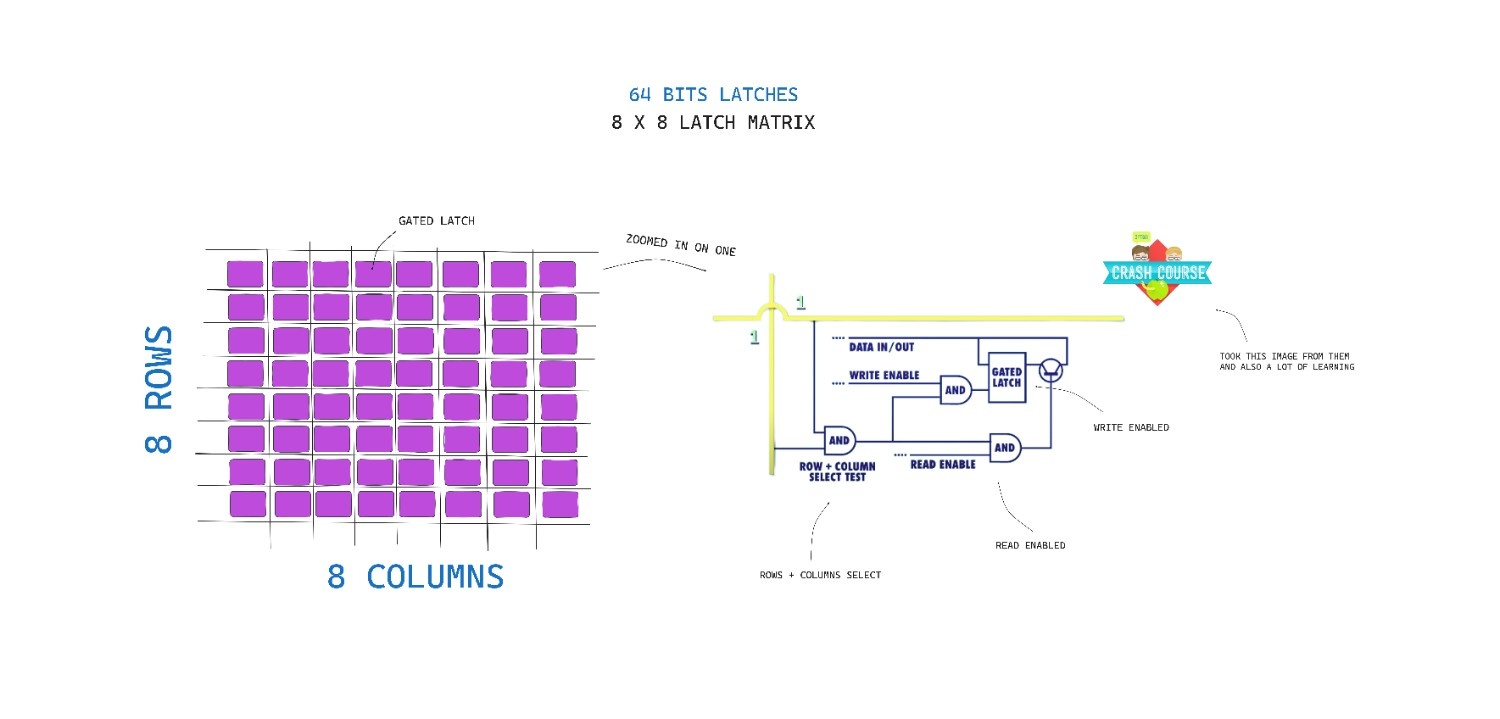
In here we arranged 64 gated latches in 8 x 8 matrix. Now let me explain you what's happening over here, I have attached a zoomed in gate so that you can understand better. There are 8 rows and 8 columns of wires, in order to activate a latch we need to activate the corresponding row and column for that latch like here you can see it is 1, 1 and this is fed to an AND gate(in draw I have mentioned it as "ROWS + COLUMNS SELECT") so this AND gate will be active if a row and a column of is active thus selecting a single latch.
This row/column setup connects all our latches with a single, shared, write enable wire. In order for a latch to become write enabled, the row wire, the column wire, and the write enable wire must all be 1. That should only ever be true for one single latch at any given time. This means we can use a single, shared wire for data. Because only one latch will ever be write enabled, only one will ever save the data the rest of the latches will simply ignore values on the data wire because they are not write enabled. We can use the same trick with a read enable wire to read the data later, to get the data out of one specific latch.
If we go by our initial setup of aligning it all in a row for 64 bits it would cost 129 wires but with this approach we reduced it to 16(8 rows + 8 columns) wires + 1 read enable wire + 1 write enable wire + 1 data in/out(to carry data) that is equal to 19 wires, we reduced it by a lot.
Now the question is how will we find the intersection now!!. We need a way to uniquely identify the intersection. So here comes the concept of addresses. We can assign addresses since we have 8 rows and 8 columns so first we need a way to store row number and column number. So how we would do it in human world lets take the first element as (1,1) then so on but in this wizarding world it only understands 0s and 1s so we just have to convert them to that. So maximum number we have to store here is 8 cause we have 8 rows. So we take 3 bits, so we can store from 0 to 7 that is 8 numbers starting from 0 we can represent each row and similary columns. So the address size will be 3 bits(to represent rows) + 3 bits(to represent columns) so total size is 6 bits. Now we can represent the first row first column latch as 000000 and first row second colum as 000001 (0 based rows and columns). Don't worry I will draw something for you and it will be more clear.
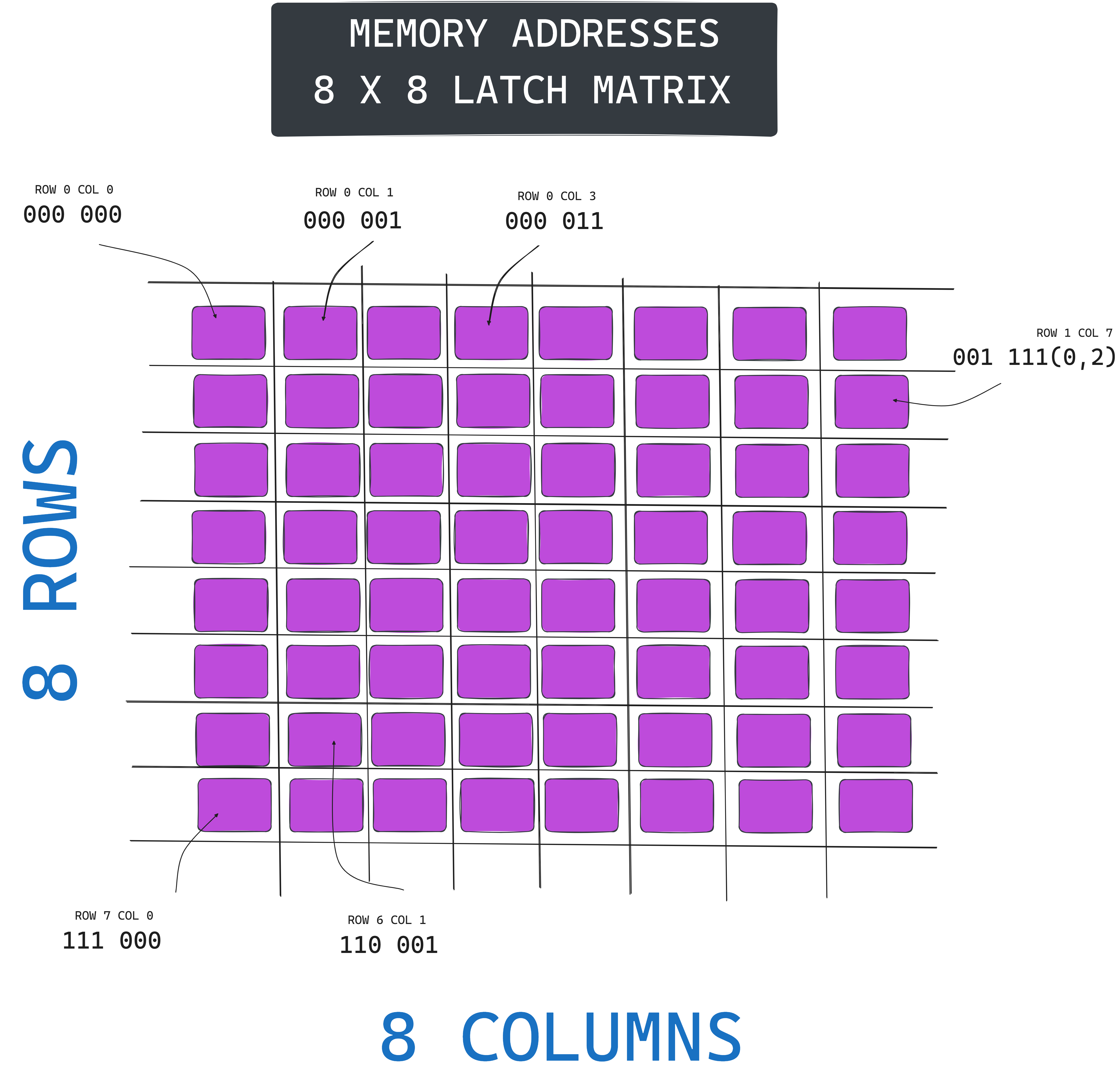
As you can see we have assigned addresses to each intersection. Now, we need something that would activate/choose/select that specific intersection, so for that we built a component called MULTIPLEXER. It simply takes in address in the form of bits and activate that corresponding address wire. So here we need a multiplexer for row and one for column. Say for example we passed 000 to row multiplexer, then it will activate the 0th row wire and same for column. Multiplexer comes in different sizes like here since we have 8 rows, we will need a 1 to 8 multiplexer cause we have 8 rows.
We have 1 to 16 and so on as well.
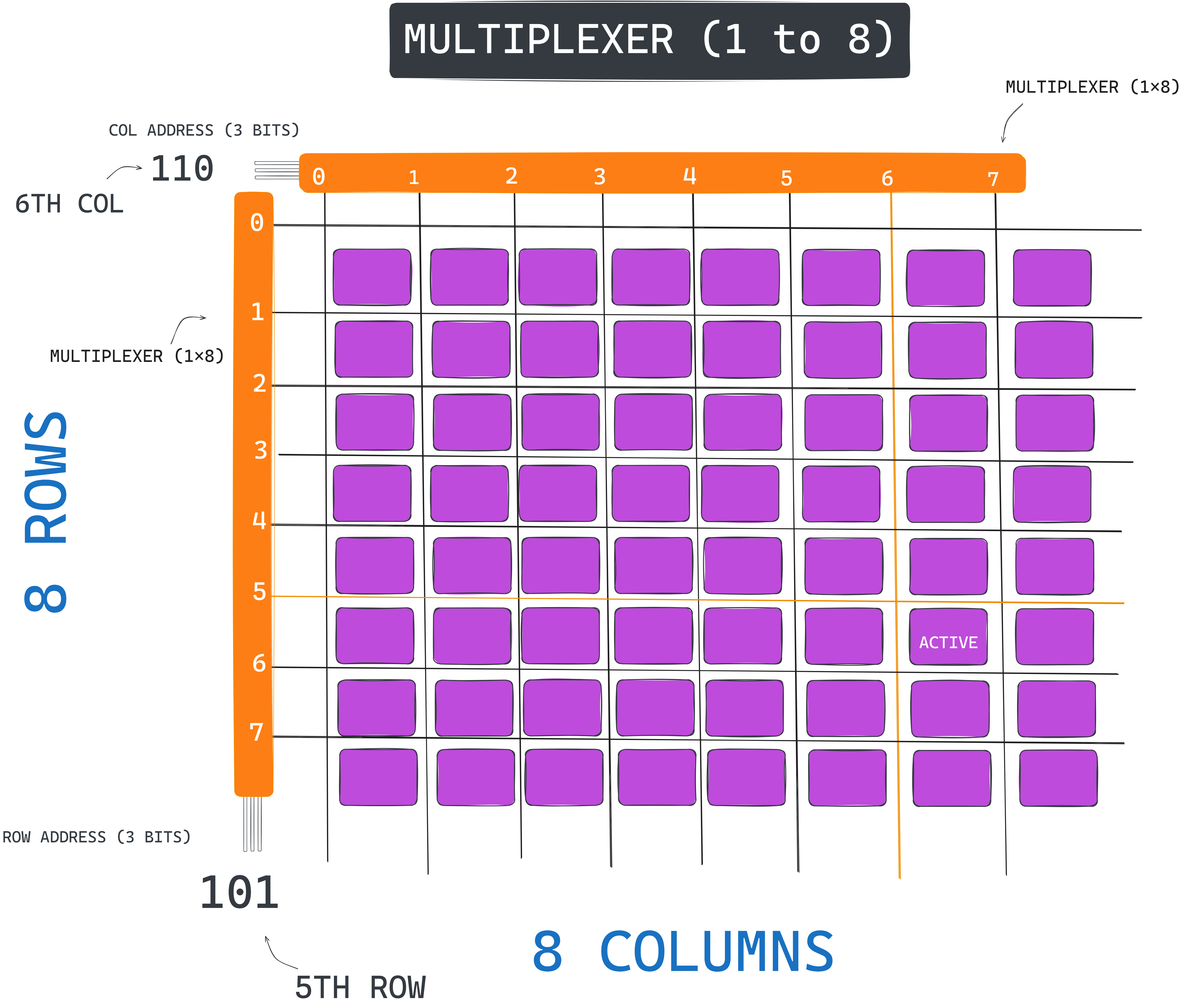
See the above draw, this is how a multiplexer works, I have specified an example as well by making 5th Row and 6th Column latch active. 64 points to Gryffindor.
64 bits for RAM is not enough, my pc has a RAM of 2 Gigabytes, we are no where close to it but it is fairly simple now that we know what we have to do. We just have to put them in a row formation again the way we did for 8 bits. and now we will have 64*8 = 512 bits of memory. Now the question is how 8-bit number is stored. So in here since we have 8 64-bits latches we can store 8 bits of number where each number will be in the same memory address. For example, for this 8 latches of 64 bit we will pass a common address to all the 8 latches and in those addresses in each latch we will store each bit. Say the number is 10010100, so now say we pass this data bits to each of the 8 latches also with the address say 110011, now every latch will have a address and a bit to store in that address and thus storing 8 bits in 8 different latches and in latches in same address location.
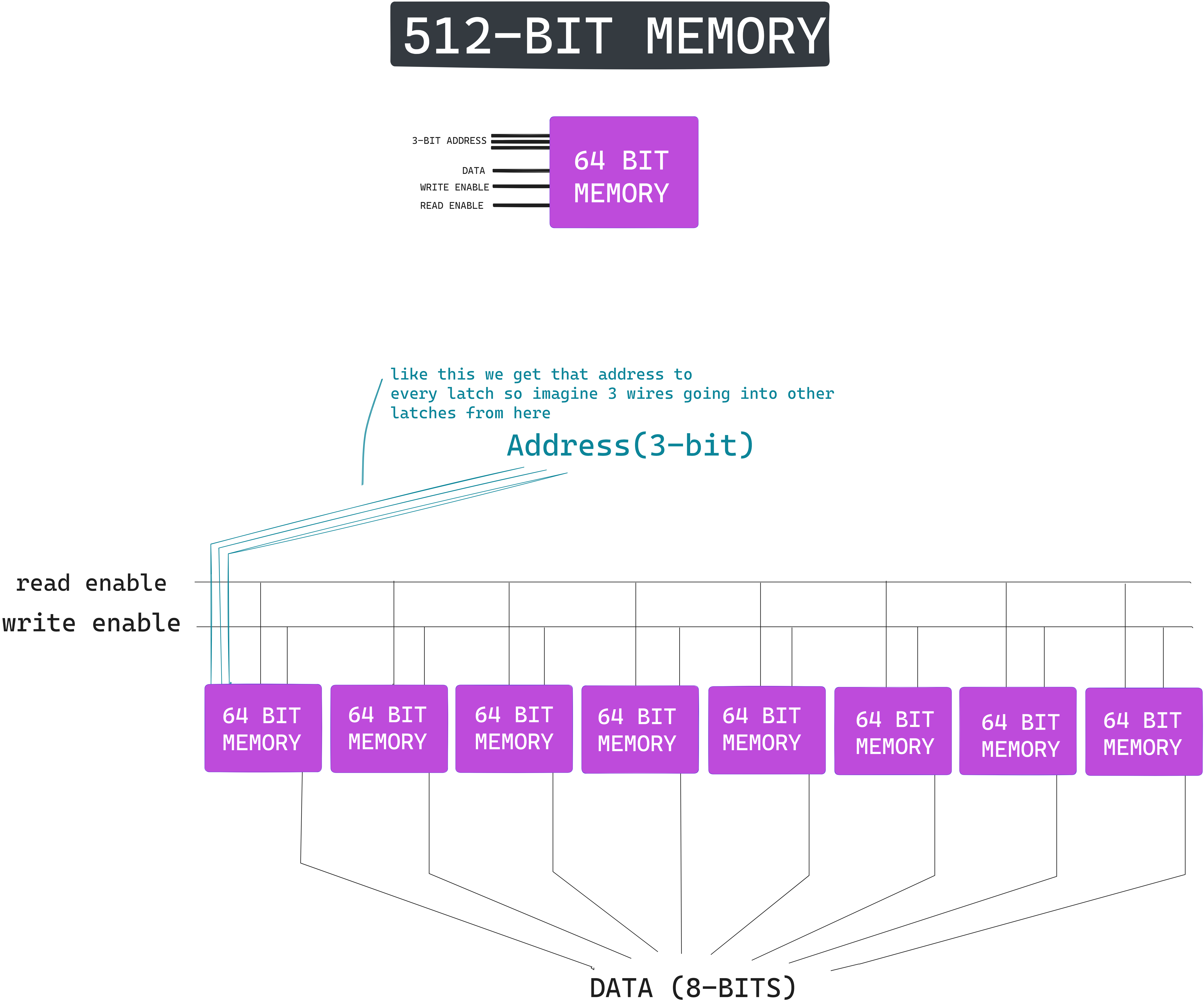
In here each bit gets to each latch's same address, we can activate write/read enable once and then write/read data from that address location.
Now the question is, it is still not close to our pc's RAM so the way modern computers scale to gigabtes and megabytes of memory is by doing the same thing we've been doing here that is keep packaging up little bundles of memory into larger and larger arrangements.
Now as the no. of locations grow, our address size will also grow. To address a gigabyte or a billion bytes of memory, we need 32 bit addresses. An important property of this memory is that we can access any memory location, at any time and in a random order. For this reason, it's called Random-Access-Memory or RAM.
This marks the end of this blog. This is my first blog and might write some more. Here is a web app that I created called Nobi which is basically link management in folder format, simply better way to manage bookmark links.
https://nobi-dusky.vercel.app/
If you want to deep dive please do visit this website, https://thecrashcourse.com/topic/computerscience/
Subscribe to my newsletter
Read articles from Vinod Murugan directly inside your inbox. Subscribe to the newsletter, and don't miss out.
Written by
