NVIDIA A100 vs V100: Which GPU is Better?
 Spheron Network
Advancements in GPU technology have transformed the landscape of memory-intensive tasks such as AI development and high-performance computing (HPC). Historically, GPUs were primarily utilized to enhance video gameplay by rendering graphics smoothly and efficiently. However, their utility has evolved significantly over time. Today, GPUs are being repurposed for more intensive computational tasks that Central Processing Units (CPUs) struggle to handle effectively.
NVIDIA has pioneered GPU technology, offering solutions that accelerate computing tasks across various domains, including gaming, scientific research, artificial intelligence (AI), and machine learning (ML). Two notable products in NVIDIA are the A100 and V100 GPUs. These GPUs cater to high-performance computing demands but are tailored to slightly different market segments and user requirements.
The A100 GPU represents one of NVIDIA's latest offerings, incorporating cutting-edge technological advancements to deliver unparalleled computing power. Conversely, the V100, although slightly older, remains a formidable option for those seeking to enhance their computational capabilities.
In this article, we will explore the intricacies of these two powerful hardware components and compare them across various dimensions, including performance, AI and ML capabilities, cost, and suitability for different applications. This comparison aims to provide insight into which GPU may best meet specific task requirements and budget considerations.
Overview of NVIDIA V100
Introduced in 2017, the NVIDIA V100 GPU established a new standard for HPC and AI acceleration. It leverages the Volta architecture, marking a significant advancement from its predecessor, Pascal, and delivering notable improvements in performance and efficiency.
Designed to meet the escalating demands of AI, machine learning, and scientific computing, the V100 addresses memory-intensive challenges. It introduced Tensor Cores, specifically tailored to accelerate AI applications, propelling the V100 beyond the 100 teraFLOPS (TFLOPS) threshold in deep learning performance.
This marked a considerable advancement from prior iterations, as the V100 integrates high-speed interconnect linking and supports extensive memory bandwidth, facilitating the efficient management and processing of large datasets.
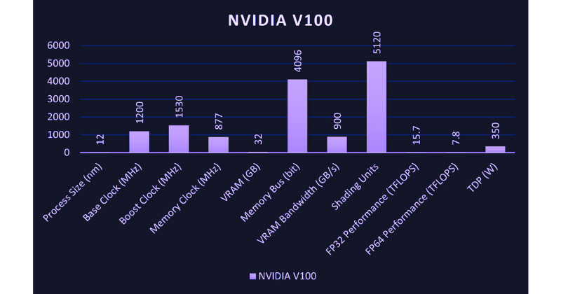
Equipped with 5,120 CUDA cores and 640 Tensor cores, the V100 offers unmatched computational prowess upon its release. It features either 32GB or 16GB of second-generation High Bandwidth Memory (HBM2), supporting memory bandwidths of up to 900 gigabytes per second (GB/s). Although the A100 surpasses its memory capacity and bandwidth, they were groundbreaking at the time of the V100's launch and remain competitive across various applications.
Furthermore, the Volta architecture, which forms the foundation of the V100, refined the Single Instruction, Multiple Threads (SIMT) execution model utilized in earlier NVIDIA architectures like Pascal.
In previous GPU architectures such as Pascal, threads were organized into groups called "warps." Each warp executed the same instruction across multiple threads. However, when different threads within a warp require different execution paths (such as due to conditional branching), inefficiencies could arise. In such cases, threads not following the "active" path had to wait, resulting in serialized execution for divergent paths and, consequently, underutilizing the GPU's computational resources.
The Volta architecture introduced an advanced iteration of the SIMT execution model, allowing for "independent thread scheduling." This enhancement enabled each thread within a warp to operate with greater independence, maintaining its own state and execution pathway without being tightly synchronized with the rest of its threads.
As a result, penalties associated with divergent code execution were reduced, as threads could diverge and converge more efficiently. This modification aimed to optimize parallel efficiency by enhancing the GPU's capability to manage divergent execution paths, which are prevalent in complex computational tasks such as those encountered in AI and HPC.
The Volta architecture's implementation of independent thread scheduling enhanced the GPU's capacity to manage intricate, fine-grained parallel algorithms more efficiently. With the V100, concurrency was enhanced, and latency related to memory-intensive operations was reduced, resulting in more effective data handling and processing.
Overview of NVIDIA A100
Debuting in May 2020, the NVIDIA A100 represents a significant advancement in GPU technology, focusing on applications within data centers and scientific computing. Built on the Ampere architecture, it offers substantial improvements over the previous Volta architecture in the V100. The A100 is meticulously engineered to cater to diverse computing tasks, spanning AI, data analytics, cloud computing, and HPC. Its design aims to elevate performance capabilities in scalable data center environments.
This implies that the A100 GPU is engineered to accelerate computing tasks across a spectrum of scenarios, ranging from isolated instances to various scales and complexities of computational workloads. This acceleration is not confined to small-scale tasks or extensive singular computations but is adaptable across different levels of computational requirements. Such scalability is pivotal in accommodating the diverse workloads data centers encounter.
The A100 surpasses its predecessor in performance and introduces several AI-specific enhancements, such as structural sparsity and Multi-Instance GPU (MIG), which enhance resource utilization and scalability.
Structural sparsity in the A100 leverages the fact that most datasets used in AI models contain many zeroes or negligible values that do not impact computation outcomes if omitted. Ignoring these unnecessary details, the A100 can execute tasks twice as fast. This optimization makes processes like training AI models and data analysis quicker and more efficient.
Conversely, MIG allows a single A100 GPU partition into multiple smaller, independent GPUs. Each instance can operate separately and handle different tasks simultaneously. This feature is especially advantageous in environments where multiple users or tasks need to share GPU resources, as it ensures optimal GPU utilization, prevents idle computational power, and scales resources according to specific needs.
What is the lifespan of the A100 GPU?
The exact lifespan of an A100 GPU depends on various factors like usage and cooling conditions. However, typically, high-end GPUs like the A100 can last for several years (5-7 years) with proper care.
Additionally, the Ampere architecture supports the latest data transfer and interconnect technologies, including PCIe Gen 4 and NVIDIA's Magnum IO, which can be integrated with Mellanox interconnect solutions. This capability allows efficient linking of multiple computers or GPUs, making it ideal for large-scale tasks requiring substantial computing power.
This versatility makes the A100 highly effective for various applications, ranging from AI training and inference to complex data analytics and high-performance computing tasks.
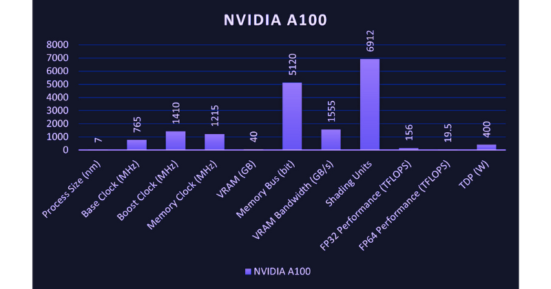
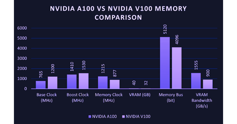
Previously, we discussed the A100's features, such as its 6,912 CUDA cores and 432 Tensor cores, enabling it to easily handle intensive data processing tasks. The GPU has 40GB of HBM2e memory, offering a bandwidth of up to 1.6 terabytes per second (TB/s), surpassing the V100's capabilities. This extensive memory and bandwidth capacity make the A100 adept at managing large datasets and complex AI models.
The A100 is designed for a broad range of use cases, from large-scale AI training and inference to HPC applications. It is a versatile solution for various high-demand computing environments.
A100 vs V100 performance comparison
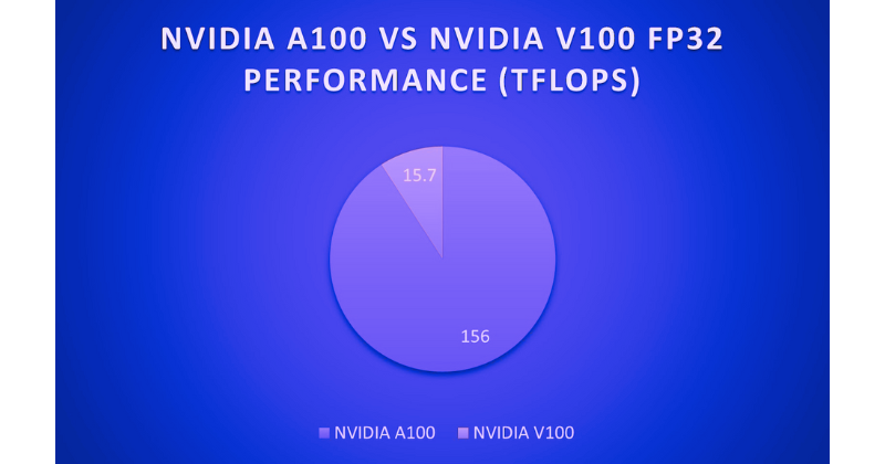
The performance comparison between NVIDIA's A100 and V100 GPUs highlights significant advancements in computational efficiency. The A100 GPU substantially improves single-precision (FP32) calculations, which are critical for deep learning and high-performance computing applications. Specifically, the A100 delivers up to 19.5 teraflops (TFLOPS), compared to the V100's 14 TFLOPS.
This increase in TFLOPS for the A100 indicates its enhanced capability to execute more floating-point calculations per second, leading to faster and more efficient processing of complex computational tasks.
Here is a table that compares both GPUs:
Specification | NVIDIA A100 | NVIDIA V100 |
Process size (nm) | 7 (Ampere architecture) | 12 (Volta architecture) |
Base clock (MHz) | 765 | 1200 |
Boost clock (MHz) | 1410 | 1530 |
Memory clock (MHz) | 1215 | 877 |
VRAM (GB) | 40 (HBM2e) | 16/32 (HBM2) |
Memory bus (bit) | 5120 | 4096 |
VRAM bandwidth (GB/s) | 1555 | 900 |
Shading units | 6912 | 5120 |
Tensor cores | Yes (3rd Gen) | Yes (2nd Gen) |
FP32 performance (TFLOPS) | Up to 156 | Up to 15.7 (single-precision) |
FP64 performance (TFLOPS) | Up to 19.5 (double-precision) | Up to 7.8 (double-precision) |
TDP (W) | 400 | 300/350 |
Manufacturing architecture | Ampere | Volta |
Target market | AI, data analytics, HPC | AI, scientific computing, HPC |
The performance difference in AI and deep learning is even more pronounced due to the A100's enhanced Tensor Cores and structural sparsity support. The A100 can achieve up to 312 TFLOPS for AI-specific tasks (using sparsity), substantially increasing over the V100's 125 TFLOPS. This makes the A100 particularly well-suited for training large, complex neural networks.
Memory performance is another critical factor in GPU comparison. The A100's 40GB of HBM2e memory offers a larger capacity than the V100’s 32GB and significantly greater bandwidth (1.6 TB/s compared to 900 GB/s). This improvement translates into better performance for data-intensive tasks and applications dealing with large datasets.
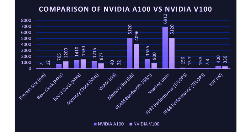
However, energy efficiency is a crucial factor, particularly in large-scale deployments. The A100 has a higher thermal design power (TDP) of approximately 400 watts, compared to the V100's 300 watts. Despite this, the performance gains delivered by the A100, especially in AI and high-performance computing tasks, make it a more energy-efficient solution overall.
The A100's superior performance in tensor operations and other AI-related computations, along with its efficient power management, enhances its performance per watt. It offers impressive computational throughput for both single-precision and tensor operations, which are essential for AI modeling and deep-learning tasks.
When considering the environmental impact and power efficiency of your GPU choice, the A100 provides significant performance advancements with only a moderate increase in power consumption. This makes it an excellent option for data centers, AI developers, and data scientists who need to balance computational demands with energy efficiency.
Suitability for different applications
While both GPUs are designed for high-performance computing, their suitability varies depending on their specifications and performance characteristics. Here is a comparison of how they perform in specific scenarios:
Scientific Research and Simulations: Both the A100 and V100 are highly capable of handling scientific research, particularly for simulations and computational tasks. However, the A100's superior performance and larger memory capacity make it more suitable for the most demanding simulations and data-intensive research projects.
Enterprise Data Analytics: For businesses that rely on large-scale data analytics, the A100 offers faster data processing and the ability to handle larger datasets. This can lead to more insightful analyses and better decision-making.
Edge Computing: While the V100 remains a solid choice for edge computing applications, the A100's advanced features and improved performance metrics provide a forward-looking solution that can better meet the increasing demands of future AI applications at the edge.
Cloud Computing and Data Centers: The A100's enhanced performance and efficiency make it particularly well-suited for cloud computing and data centers, where scalability and energy efficiency are crucial. Its ability to handle multiple tasks simultaneously allows for more flexible and cost-effective cloud services.
A100 vs. V100 cost and value analysis
The cost of GPUs is a crucial factor for many users, influencing their overall value across different market segments.
Initial Costs and Availability: The A100 is generally more expensive than the V100, reflecting its newer technology and higher performance capabilities. However, prices can vary based on supply and demand, as well as specific configurations and models.
Total Cost of Ownership: When considering the total cost of ownership, it's important to account for both the initial purchase price and operating costs, such as power consumption and cooling. The A100's improved energy efficiency can lead to lower long-term costs, potentially offsetting its higher initial price for many users.
Future-proofing and longevity
Considering the rapid pace of technological advancement, future-proofing is essential for organizations investing in high-performance computing solutions.
Evolving Computational Needs: The A100 is better positioned to meet the increasing demands of future computational tasks and AI algorithms, thanks to its newer architecture and higher performance. This makes it a more future-proof investment, potentially offering a longer lifespan before becoming obsolete.
NVIDIA’s Support and Updates: NVIDIA provides extensive support for both GPUs, including driver updates and optimizations. However, as a newer product, the A100 is likely to receive longer-term support and more frequent updates, enhancing its longevity.
Resale Value and Demand: The demand for high-performance GPUs in the secondary market can affect their resale value. The A100, being newer and more powerful, is likely to maintain a higher resale value over time compared to the V100.
The NVIDIA A100 and V100 GPUs offer exceptional performance and capabilities tailored to high-performance computing, AI, and data analytics. The A100 stands out for its advancements in architecture, memory, and AI-specific features, making it a better choice for the most demanding tasks and future-proofing needs. However, the V100 remains a viable and cost-effective option for many applications, especially for those with less stringent performance requirements or budget constraints.
Ultimately, the choice between the A100 and V100 will depend on individual needs, budget, and the specific applications envisioned. As GPU technology continues to evolve, staying informed about the latest developments and how they align with your computational needs will be key to making the most informed decision.
Subscribe to my newsletter
Read articles from Spheron Network directly inside your inbox. Subscribe to the newsletter, and don't miss out.
Written by

Spheron Network
Spheron Network
On-demand DePIN for GPU Compute