How a Program Runs
 Ahmed Gouda
Translate a C Program into a Machine Program
Compilers
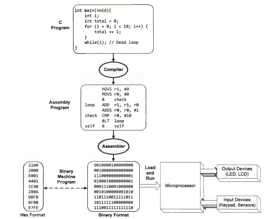
Compilers translate a human-readable source program written in a high-level programming language, such as C, into a low-level machine-understandable executable file encoded in binary form. Executable files created by compilers are usually platform dependent.
Compilers first perform some analysis on the source program, such as:
Extracting Symbols
Checking Syntax
then creates an intermediate representation (IR).
Compilers make some transformations and optimizations to the IR to improve the program execution speed or reduce the program size.
For C compilers, the intermediate program is similar to an assembly program. Finally, compilers translate the assembly program into a machine program, also called a binary executable, which can run on the target platform. The machine program consists of computer instructions and data symbols.
Assembly Program
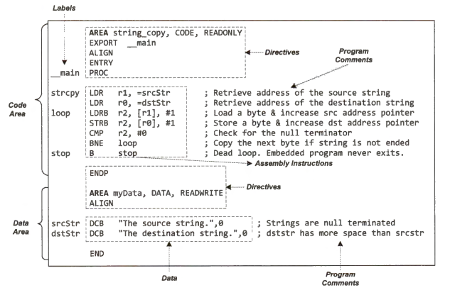
An assembly program includes the following five key components:
Label: represents the memory address of a data variable or an assembly instruction.
Instruction Mnemonic: an operation that the processor should perform, such as " ADD" for adding integers.
Operands of a machine operation can be numeric constants or processor registers.
Program Comment aims to improve inter-programmer communication and code readability by explicitly specifying programmers' intentions, assumptions, and hidden concepts.
Assembly Directive is not a machine instruction, but it defines the data content or provides relevant information to assist the assembler.
Binary Machine Program
The binary machine program follows a standard called Executable and Linkable Format (ELF), which most Linux and UNIX systems use. The UNIX System Laboratories developed and published ELF to standardize the format for most executable files, shared libraries, and object code.
Object code is an intermediate file that a compiler generates at the compiling stage. Compilers link object code together at the linking stage to form an executable or a software library.
ELF provides two interfaces to binary files:
Linkable Interface: This is used at static link time to combine multiple files when compiling and building a program.
Executable Interface: This is utilized at runtime to create a process image in memory when a program is loaded into memory and then executed.
Below is the interface of an executable binary file in the executable and linking format (ELF).
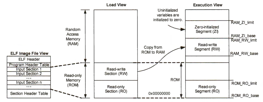
In ELF, similar data, symbols, and other information are grouped into many important input sections.
The executable interface provides two separate logic views:
Load View
Specifies how to load data into the memory.
Classifies the input sections into two regions:
Read-Write section.
Read-Only section.
Defines the base memory address of these regions.
So that the processor knows where it should load them into the memory.
Execution View
Instructs how to initialize data regions at runtime.
Informs the processor how to load the executable at runtime.
A binary machine program includes four critical sections, including:
text segment: consists of binary machine instructions
read-only data segment: defines the value of variables unalterable at runtime.
read-write data segment: sets the initial values of statically allocated and modifiable variables.
zero-initialized data segment: holds all uninitialized variables declared in the program.
Load a Machine Program into Memory
Binary executable programs are initially stored in non-volatile storage devices such as hard drives and flash memory. Therefore, when the system loses power, the program is not lost, and the system can restart. The processor must load the instructions and data of a machine program into main memory before the program starts to run. Main memory usually consists of volatile data storage devices, such as DRAM and SRAM, and all stored information in main memory is lost if power is turned off.
Harvard Architecture and Von Neumann Architecture
There are two types of computer architecture:
Von Neumann architecture
Harvard architecture
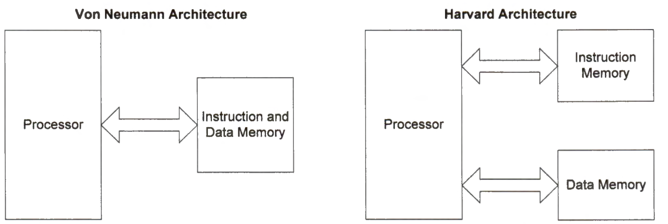
In the Von Neumann architecture, data and instructions share the same physical memory. There are only one memory address bus and one data transmission bus. A bus is a communication connection, which allows the exchange of information between two or more parts of a computer. All sections of an executable program, including the text section (executable instructions), the read-only data section, the read-write sections, and the zero-initialized section, are loaded into the main memory. The data stream and the instruction stream share the memory bandwidth.
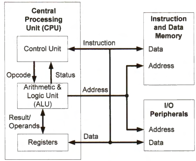
In the Harvard architecture, the instruction memory and data memory are two physically separate memory devices. There are two sets of data transmission buses and memory address buses. When a program starts, the processor copies at least the read-write data section and the zero-initialized data section in the binary executable to the data memory. Copying the read-only data section to the data memory is optional. The text section usually stays in the non-volatile storage. When the program runs, the instruction stream and the data stream transfer information on separate sets of data and address buses.
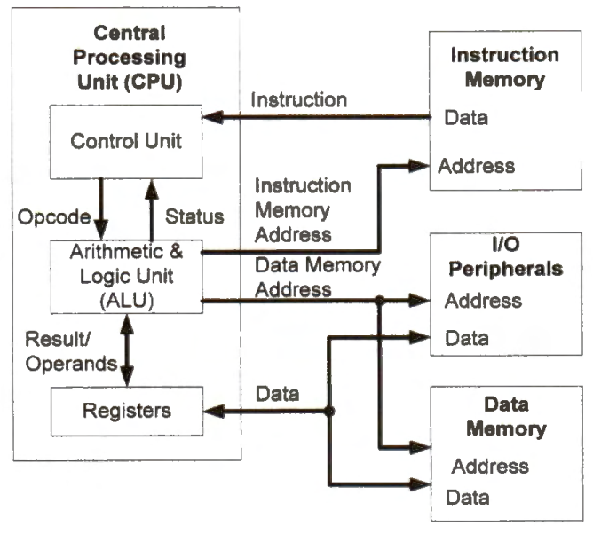
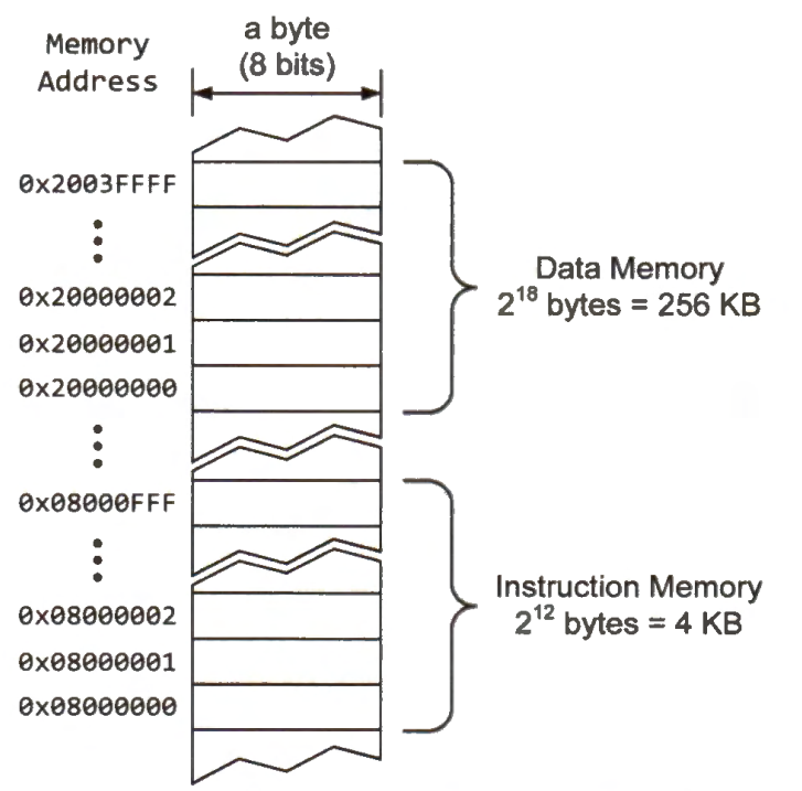
In the Harvard architecture, the instruction memory and the data memory are often small enough to fit in the same address space. For a 32-bit processor, the memory address has 32 bits. Modern computers are byte-addressable (i.e., each memory address identifies a byte in memory). When the memory address has 32 bits, the total addressable memory space includes 2^32 bytes (i.e., 4 GB). A 4-GB memory space is large enough for embedded systems.
Because the data and instruction memory are small enough to fit in the same 32-bit memory address space, they often share the memory address bus, as shown in Figure 1-5. Suppose the data memory has 256 kilobytes 2^18 bytes, and the instruction memory has 4 kilobytes 2^12 bytes. In the 32-bit (i.e., 4 GB) memory address space, we can allocate a 4KB region for the instruction memory and a 256KB region for the data memory. Because there is no overlap between these two address ranges, the instruction memory and the data memory can share the address bus.
Each type of computer architecture has its advantages and disadvantages.
The Von Neumann architecture is relatively inexpensive and simple.
The Harvard architecture allows the processor to access the data memory and the instruction memory concurrently. By contrast, the Von Neumann architecture allows only one memory access at any time instant; the processor either reads an instruction from the instruction memory or accesses data in the data memory. Accordingly, the Harvard architecture often offers faster processing speed at the same clock rate.
The Harvard architecture tends to be more energy efficient. Under the same performance requirement, the Harvard architecture often needs lower clock speeds, resulting in a lower power consumption rate.
In the Harvard architecture, the data bus and the instruction bus may have different widths. For example, digital signal processing processors can leverage this feature to make the instruction bus wider to reduce the number of clock cycles required to load an instruction.
Creating Runtime Memory Image
ARM Cortex-M3/M4/M7 microprocessors are Harvard computer architecture, and the instruction memory (flash memory) and the data memory (SRAM) are built into the processor chip.
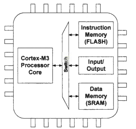
The microprocessor employs two separate and isolated memories. Separating the instruction and data memories allows concurrent access to instructions and data, thus improving the memory bandwidth and speeding up the processor performance. Typically, the instruction memory uses a slow but nonvolatile flash memory, and the data memory uses a fast but volatile SRAM.
The below figure gives a simple example that shows how the Harvard architecture loads a program to start the execution. When the processor loads a program, all initialized global variables, such as the integer array a, are copied from the instruction memory into the initialized data segment in the data memory. All uninitialized global variables, such as the variable counter, are allocated in the zero-initialized data segment. The local variables, such as the integer array b, are allocated on the stack, located at the top of SRAM. Note the stack grows downward. When the processor boots successfully, the first instruction of the program is loaded from the instruction memory into the processor, and the program starts to run.
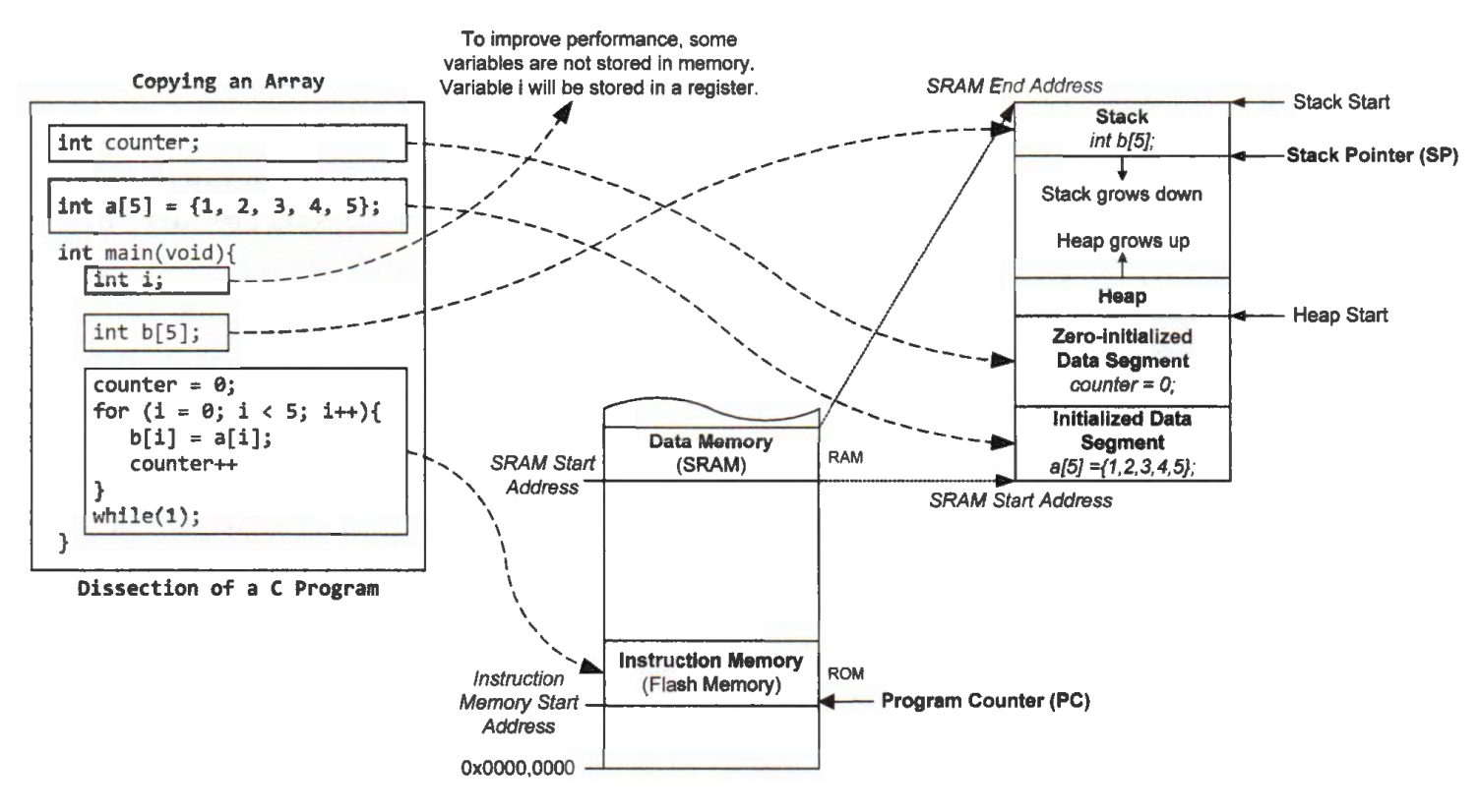
At runtime, the data memory is divided into four segments:
initialized data segment
uninitialized data segment
heap
stack
The processor allocates the first two data segments statically, and their size and location remain unchanged at runtime. The size of the last two segments changes as the program runs.
Initialized Data Segment
The initialized data segment contains global and static variables that the program gives some initial values. For example, in a C declaration int capacity = 100;, if it appears outside any function (global variable), the processor places the variable capacity in the initialized data segment with an initial value when the processor creates a running time memory image for this C program.
Uninitialized (Zero-Initialized) Data Segment
The zero-initialized data segment contains all global or static variables that are uninitialized or initialized to zero in the program. For example, a globally declared string char name [20]; is stored in the uninitialized data segment.
Heap
The heap holds all data objects that an application creates dynamically at runtime. For example, all data objects created by dynamic memory allocation library functions like malloc() or calloc() are placed in the heap. A free() function removes a data object from the heap, freeing up the memory space allocated to it. The heap is placed immediately after the zero-initialized segment and grows upward (toward higher addresses).
Stack
The stack stores local variables of subroutines, including main(), saves the runtime environment, and passes arguments to a subroutine. A stack is a first-in-last-out (FILO) memory region, and the processor places it on the top of the data memory. When a subroutine declares a local variable, the variable is saved in the stack. When a subroutine returns, the subroutine should pop from the stack all variables it has pushed. Additionally, when a caller calls a subroutine, the caller may pass parameters to the subroutine via the stack. As subroutines are called and returned at runtime, the stack grows downward or shrinks upward correspondingly.
.
The processor places the heap and the stack at the opposite end of a memory region, and they grow in different directions. In a free memory region, the stack starts from the top, and the heap starts from the bottom. As variables are dynamically allocated or removed from the heap or stack, the size of the heap and stack changes at runtime. The heap grows up toward the large memory address, and the stack grows down toward the small memory address. Growing in opposite directions allows the heap and stack to take full advantage of the free memory region. When the stack meets the heap, free memory space is exhausted.
The figure below shows an example memory map of the 4GB memory space in a Cortex-M3 microprocessor. The memory map is usually pre-defined by the chip manufacturer and is not programmable. Within this 4GB linear memory space, the address range of instruction memory, data memory, internal and external peripheral devices, and external RAM does not overlap with each other.
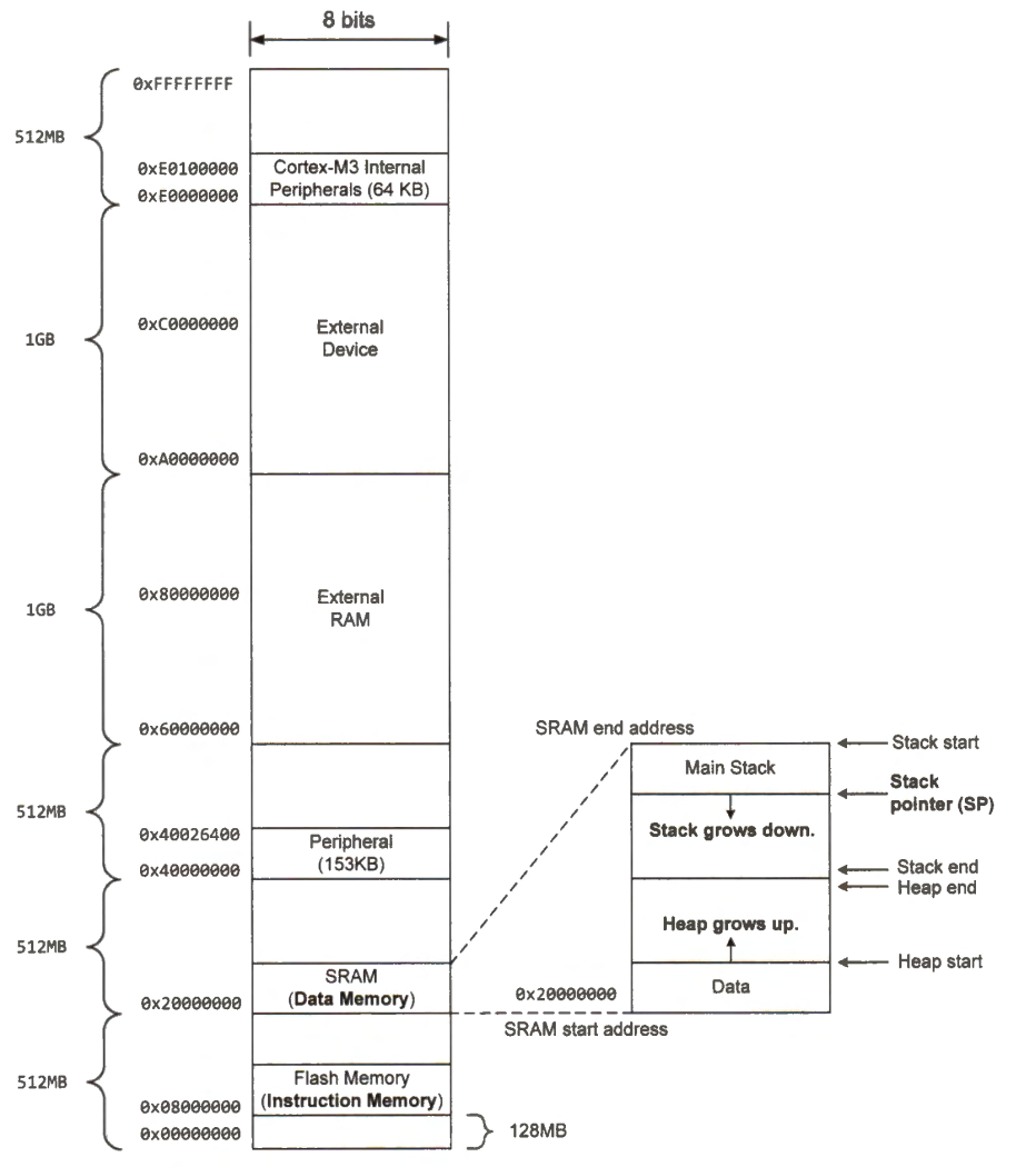
The on-chip flash memory, used for the instruction memory, has 4 KB, and its address starts at 0x08000000.
The on-chip SRAM, used for the data memory, has 256 KB, and its memory address begins at 0x20000000.
The external RAM allows the processor to expand the data memory capacity.
The processor allocates memory addresses for each internal or external peripheral. This addressing scheme enables the processor to interface with a peripheral in a convenient way. A peripheral typically has a set of registers, such as data registers for data exchange between the peripheral and the processor, control registers for the processor to configure or control the peripheral, and status registers to indicate the operation state of the peripheral. A peripheral may also contain a small memory.
The processor maps the registers and memory of all peripherals to the same memory address space as the instruction and data memory. To interface a peripheral, the processor uses regular memory access instructions to read or write to memory addresses predefined for this peripheral. This method is called memory-mapped I/O. The processor interfaces all peripherals as if they were part of the memory.
Registers
Before we illustrate how a microprocessor executes a program, let us first introduce one important component of microprocessors - hardware registers. A processor contains a small set of registers to store digital values. Registers are the fastest data storage in a computing system.
All registers are of the same size and typically hold 16, 32, or 64 bits. Each register in Cortex-M processors has 32 bits. The processor reads or writes all bits in a register together. It is also possible to check or change individual bits in a register. A register can store the content of an operand for a logic or arithmetic operation, or the memory address or offset when the processor access data in memory.
A processor core has two types of registers:
general-purpose registers
special-purpose registers
While general-purpose registers store the operands and intermediate results during the execution of a program, special-purpose registers have a predetermined usage, such as representing the processor status. Special-purpose registers have more usage restrictions than general-purpose registers. For example, some of them require special instructions or privileges to access them.
A register consists of a set of flip-flops in parallel to store binary bits. A 32-bit register has 32 flip-flops side by side. Below is a simple implementation of a flip-flop by using a pair of NAND gates. A flip-flop usually has a clock input, which is not shown in this example.

The flip-flop works as follows. When the set or the reset is true, a digital value of 1 or 0 is stored, respectively. When both the set and the reset are true, the digital value stored remains unaffected. The set and reset signals cannot be false simultaneously. Otherwise, the result produced would be random.
Reusing Registers to Improve Performance
Accessing the processor's registers is much faster than data memory. Storing data in registers instead of memory improves the processor performance.
In most programs, the probability that a data item is accessed is not uniform. It is a common phenomenon that a program accesses some data items much more frequently than the other items. Moreover, a data item that the processor accesses at one point in time is likely to be accessed again shortly. This phenomenon is pervasive in applications, and it is called temporal locality. Therefore, most compilers try to place the value of frequently or recently accessed data variables and memory addresses in registers whenever possible to optimize the performance.
Software programs also have spatial locality. When a processor accesses data at a memory address, data stored in nearby memory locations are likely to be read or written shortly. Processor architecture design (such as caching and prefetching) and software development (such as reorganizing data access sequence) exploit spatial locality to speed up the overall performance.
The number of registers available on a microprocessor is often small, typically between 4 and 32, for two important reasons.
Many experimental measurements have shown that registers often exhibit the highest temperature compared to the other hardware components of a processor. Reducing the number of registers helps mitigate the thermal problem.
If there are fewer registers, it takes fewer bits to encode a register using machine instructions. A small number of registers consequently decrease the code size and reduce the bandwidth requirement on the instruction memory. For example, if a processor has 16 registers, it requires 4 bits to represent a register in an instruction. To encode an assembly instruction with two operand registers and one destination register, such as
add r3, rl, r2 (r3 = rl + r 2), the binary machine instruction uses 12 bits to identify these registers. However, if a processor has only eight registers, encoding three registers in an instruction takes only 9 bits.
Register Allocation
Register allocation is a process that assigns variables and constants to general-purpose registers. A program often has more variables and constants than registers. Register allocation decides whether a variable or constant should reside in a processor register or at some location in the data memory. Register allocation is performed either automatically by compilers if the program is written in a high-level language (such as C or C++) or manually if the program is in assembly.
Finding the optimal register allocation that minimizes the number of memory accesses is a very challenging problem for a given program. Register allocation becomes further complicated in Cortex-M processors. For example, some instructions can only access registers with small addresses (low registers). Some instructions, such as multiplication, place a 64-bit result into two registers.
When writing an assembly program, we can follow three basic steps to allocate registers.
We inspect the live range of a variable. A variable is live if the program accesses it again at some later point in time.
If the live ranges of two variables overlap, we should not allocate them to the same register. Otherwise, we can assign them to the same register.
We map the most frequently used variables to registers and allocate the least frequently used variables in the data memory, if necessary, to reduce the number of memory accesses.
Processor Registers
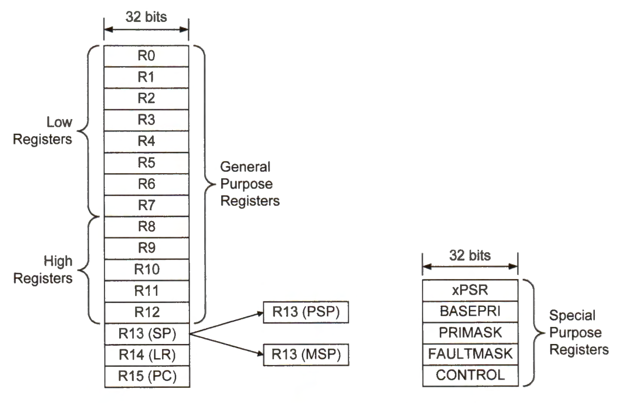
Processor registers are divided into two groups: general-purpose registers and special-purpose registers. Register names are case-insensitive.
General Purpose Registers
There are 13 general-purpose registers (r0 - r12) available for program data operations. The first eight registers (r0 - r7) are called low registers, and the other five (r8 - r12) are called high registers.
Some of the 16-bit assembly instructions in Cortex-M can only access the low registers.
Special Purpose Registers
Stack point (SP) r13
Holds the memory address of the top of the stack. Cortex-M processors provide two different stacks: the main stack and the process stack.
Thus, there are two stack pointers: the main stack pointer (MSP) and the process stack pointer (PSP).
The processor uses PSP when executing regular user programs and uses MSP when serving interrupts or privileged accesses.
The stack pointer SP is a shadow register of either MSP or PSP, depending on the processor's mode setting. When a processor starts, it assigns MSP to SP initially.Link register (LR) r14
Holds the memory address of the instruction that needs to run immediately after a subroutine completes. It is the next instruction after the instruction that calls a subroutine. During the execution of an interrupt service routine, LR holds a special value to indicate whether MSP or PSP is used.Program counter (PC) r15
Holds the memory address (location in memory) of the next instruction(s) that the processor fetches from the instruction memory.Program status register (xPSR)
Records status bit flags of the application program, interrupt, and processor execution.
Example flags include negative, zero, carry, and overflow.Base priority mask register (BASEPRI)
Defines the priority threshold, and the processor disables all interrupts with a higher priority value than the threshold. A lower priority value represents a higher priority (or urgency).Control register (CONTROL)
Sets the choice of the main stack or the process stack and the selection of privileged or unprivileged mode.Priority mask register (PRIMASK)
Used to disable all interrupts excluding hard faults and non-maskable interrupts (NMI). If an interrupt is masked, the processor disables this interrupt.Fault mask register (FAULTMASK)
Used to disable all interrupts excluding non-maskable interrupts (NMI).
The program counter (PC) stores the memory address at which the processor loads the next instruction(s). Instructions in a program run sequentially if the program flow is not changed. Usually, the processor fetches instructions consecutively from the instruction memory. Thus, the program counter is automatically incremented, pointing to the next instruction to be executed.
PC = PC + 4 after each instruction fetch
Each instruction in Cortex-M has either 16 or 32 bits. Typically, the processor increases the program counter by four automatically. The processor retrieves four bytes from the instruction memory in one clock cycle. Then the processor decodes these 32 bits and finds out whether they represent one 32-bit instruction or two 16-bit instructions.

Normally, assembly instructions in a program run in a sequential order. However, branch instructions, subroutines, and interrupts can change the sequential program flow by setting the PC to the memory address of the target instruction.
Instruction Lifecycle
For Cortex-MO/M3/M4, each instruction takes three stages:
At the first stage, the processor fetches 4 bytes from the instruction memory and increments the program counter by 4 automatically. After each instruction fetch, the program counter points to the next instruction(s) to be fetched.
At the second stage, the processor decodes the instruction and finds out what operations are to be carried out.
At the last stage, the processor reads operand registers, carries out the designated arithmetic or logic operation, accesses data memory (if necessary), and updates target registers (if needed).
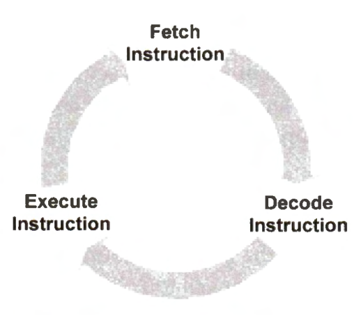
This fetch-decode-execution process repeats for each instruction until the program finishes.
The processor executes each instruction in a pipelined fashion, like an automobile assembly line. Pipelining allows multiple instructions to run simultaneously, increasing the utilization of hardware resources and improving the processor's overall performance. To execute programs correctly, a pipeline processor should take special considerations to branch instructions. For example, when a branch instruction changes the program flow, any instructions that the processor has fetched incorrectly should not complete the pipeline.

While Cortex-MO, Cortex-M3, and Cortex-M4 have three pipeline stages, Cortex-MO+ has only two stages, including instruction fetch and execution. As well, Cortex-MO+ is based on Von Neumann Architecture, instead of Harvard Architecture. Cortex-M7 is much more complicated, and it has multiple pipelines, such as load/store pipeline, two ALU pipeline, and FPU pipeline. It allows more instructions to run concurrently. Each pipeline can have up to six stages, including instruction fetch, instruction decode, instruction issue, execute sub-stage 1, execute sub-stage 2, and write back.
Executing a Machine Program
This section illustrates how a Cortex-M processor executes a program. We use a simple C program. The program calculates the sum of two global integer variables (a and b) and saves the result into another global variable c. Because most software programs in embedded systems never exit, there is an endless loop at the end of the C program.
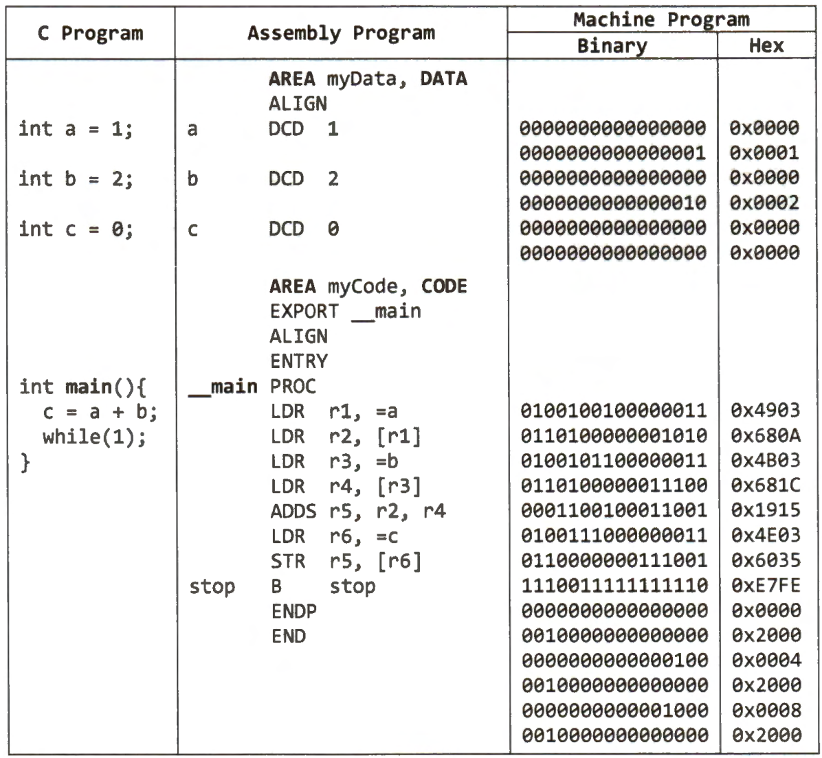
A compiler translates the C program into an assembly program. Different compilers may generate assembly programs that differ from each other. Even the same compiler can generate different assembly programs from the same C program if different compilation options (such as optimization levels) are used.
The assembler then produces the machine program based on the assembly program.
The machine program includes two parts: data and instructions.
The above table only lists the instructions.
Note that the assembly program uses instruction ADDS rs, r2, r4, instead of ADD rs, r2, r4, even though the processor does not use the N, Z, C, and V flags updated by the ADDS instruction in this program. The ADD instruction has 32 bits, and ADDS has only 16 bits. The compiler prefers ADDS to ADD to reduce the binary program size.
Loading a Program
When the program runs on Harvard architecture, its instructions and data are loaded into the instruction and data memory, respectively.
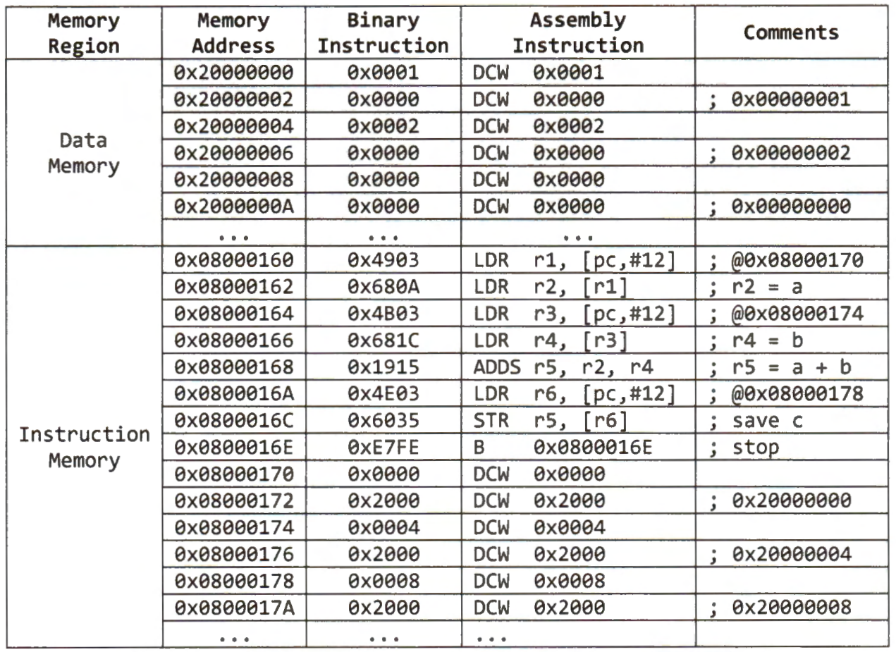
Depending on the processor hardware setting, the starting address of the instruction and data memory might differ from this example. Each instruction in this example happens to take two bytes in the instruction memory. The global variables are placed in the data memory when a program runs.
By default, the address of the RAM, used as data memory, starts at 0x20000000. Therefore, these three integer variables (a, b, and c) are stored in the RAM, and their starting address is 0x20000000. Each integer takes four bytes in memory.
Each instruction takes three clock cycles (fetch, decode, and execute) to complete on ARM Cortex-M3 and Cortex-M4 processors:
Fetch the instruction from the instruction memory,
Decode the instruction, and
Execute the arithmetic or logic operation,
update the program counter for a branch instruction,
or access the data memory for a load or store instruction.
The assembly instruction LDR r1, =a is a pseudo instruction, and the compiler translates it to a real machine instruction. This instruction sets the content in register r1 to the memory address of variable a. The pseudo instruction is translated toLDR r1, [pc, #12]. The memory address of variable a is stored at the memory location [pc, #12]. This PC-relative addressing scheme is a general approach to loading a large irregular constant number into a register.
Starting Execution
After the processor is booted and initialized, the program counter (PC) is set to 0x08000160. After executing an instruction, the processor increments the PC automatically by four. PC points to the next 32-bit instruction or the next two 16-bit instructions to be fetched from the instruction memory. In this example, each instruction takes only two bytes (16 bits), but many instructions take four bytes (32 bits).
Each processor has a special program called boot loader, which sets up the runtime environment after completion of self-testing. The boot loader sets the PC to the first instruction of a user program. For a C program, PC points to the first statement in the main function. For an assembly program, PC points the first instruction of the __main function.
The below figure shows the values of registers, the layout of instruction memory and data memory after the processor loads the sample program. When the program starts, PC is set to 0x08000160. Note each memory address specifies the location of a byte in memory. Because each instruction takes 16 bits in this example, the memory address of the next instruction is 0x08000162. Variables a, b, and care are declared as integers, and each of them takes four bytes in memory.
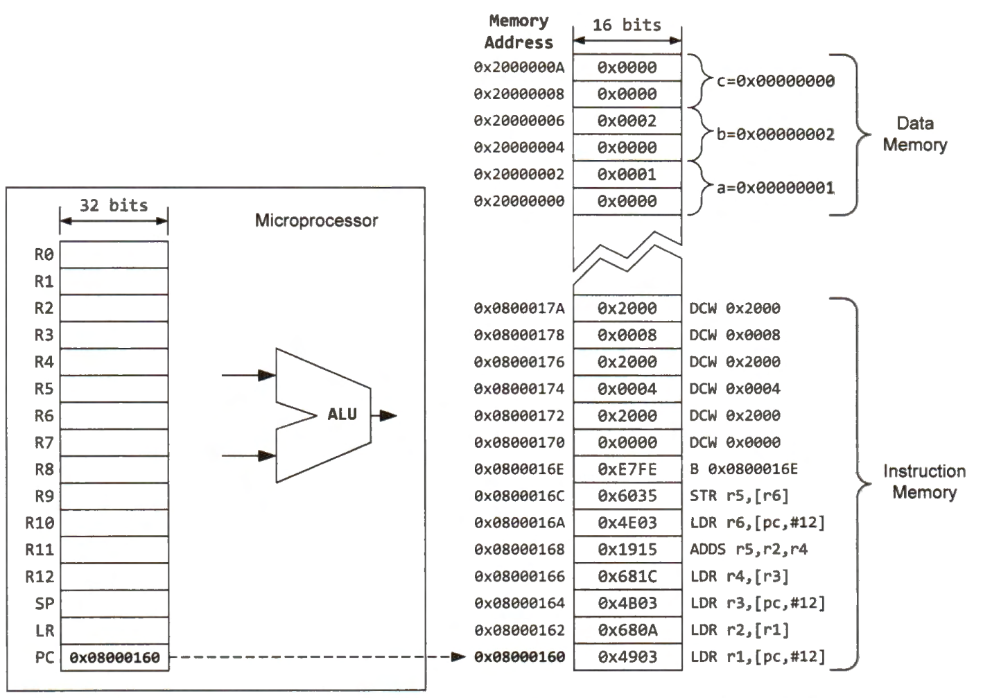
Registers hold values to be operated by the arithmetic and logic unit (ALU). All registers can be accessed simultaneously without causing any extra delay. A variable can be stored in memory or a register. When a variable is stored in the data memory, the value of this variable must be loaded into a register because arithmetic and logic instructions cannot directly operate on a value stored in memory. The processor must carry out the load-modify-store sequence to update this variable:
Load the value of the variable from the data memory into a register,
Modify the value of the register by using ALU,
Store the value of this register back into the data memory.
The previously mentioned assembly program involves the following four key steps:
Load the value of variable a from the data memory into register r2.
Load the value of variable b from the data memory into register r4.
Calculate the sum of r2 and r4 and save the result into register r5.
Save the content of register r5 to the memory where variable c is stored.
Program Completion
The below figure shows the values of all registers and the data memory when the program reaches the dead loop.
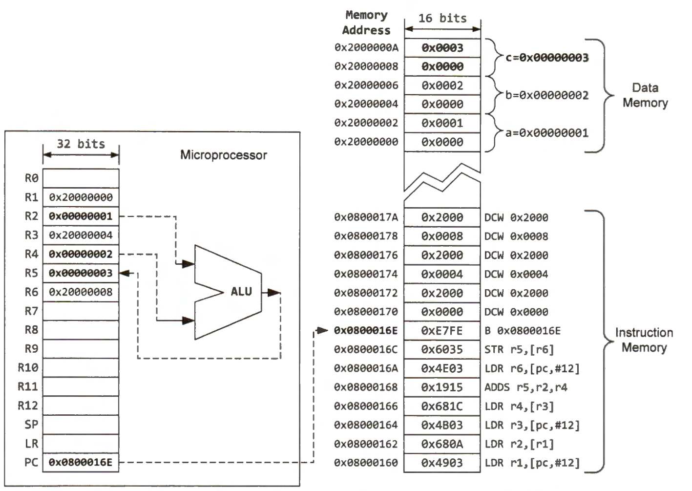
The instruction memory remains unchanged because it is read-only.
The data memory stores computed values that may change at run time.
The program saves the result in the data memory. Variable c stored at the data memory address 0x20000008 has a value of 3, which is the sum of a and b.
The program counter (PC) is kept at 0x0800016E, pointing to the instruction 0xE7F E repeatedly. PC keeps pointing to the current instruction, which forms a dead loop. In embedded systems, most applications do not return and consequently place a dead loop at the end of the main function.
During the computation, values stored in the data memory cannot be operands of ALU directly. To process data stored in the data memory, the processor must load data into the processor's general-purpose registers first. Neither can the processor save the result of ALU to the data memory directly. The processor should write the ALU result to a general-purpose register first and use a store instruction to copy the data from the register to the data memory.
Subscribe to my newsletter
Read articles from Ahmed Gouda directly inside your inbox. Subscribe to the newsletter, and don't miss out.
Written by

Ahmed Gouda
Ahmed Gouda
Embedded Software Engineer who are interested in Embedded Systems Design, Embedded Software, Electrical Engineering, and Electronics, C\C++ programming, Assembly, Computer Architecture, Microprocessors, Microcontrollers, and Communication Protocols.