AMD Prepares Memory Instinct M1325X for End of 2024, Shares 2026 Accelerator Roadmap
 Spheron Network
At this year’s Computex trade show, AMD CEO Dr. Lisa Su devoted significant attention to AI during her keynote presentation. While much of the focus was on AMD's upcoming client products, the company is also experiencing rapid growth in its Instinct accelerator lineup. The MI300 continues to exceed sales expectations and set new growth records each quarter. This momentum drives AMD to advance swiftly in the AI accelerator market to seize opportunities and remain competitive against numerous chipmakers.
As part of the announcements, AMD unveiled their Instinct product roadmap, detailing plans for both short-term and long-term developments through 2026 and beyond.
On the product front, AMD introduced the new Instinct accelerator, the MI325X, which features HBM3E memory. The MI325X is based on the same computational technology as the MI300X. Still, it replaces HBM3 memory with the faster and denser HBM3E, resulting in accelerators with up to 288GB of memory and local memory bandwidths reaching 6TB/second.
AMD presented its first new CDNA architecture/Instinct product roadmap in two years, outlining its strategy through 2026. Over the next two years, AMD plans to launch two new CDNA architectures and corresponding Instinct products in 2025 and 2026. The CDNA 4-powered MI350 series is set for release in 2025, followed by the ambitious MI400 series, based on the CDNA "Next" architecture.
AMD Instinct MI325X: The Ultimate Memory Beast
To begin, let’s examine AMD’s newly updated MI325X accelerator. Like other vendors like NVIDIA with their H200, AMD is launching a mid-generation refresh of the MI300X accelerator, leveraging the new HBM3E memory. HBM3E, an update to the HBM standard, offers higher clock speeds and greater memory densities.
Using 12-Hi stacks, all three major memory vendors are (or will be) producing 36GB of memory, a 50% increase over the current 24GB HBM3 stacks. This enhancement allows the MI300 series, with its 8-stack configuration, to boost its maximum memory capacity from 192GB to an impressive 288GB on a single accelerator.
Additionally, HBM3E brings faster memory clock speeds. Micron and SK Hynix are expected to sell stacks clocking up to 9.2Gbps/pin, while Samsung aims for 9.8Gbps/pin—over 50% faster than the 6.4Gbps data rate of standard HBM3 memory. Although it remains to be seen when products using these speeds will emerge (as no accelerator has yet run HBM3 at 6.4Gbps), HBM3E will provide chip vendors with much-needed memory bandwidth.
Here is a comparison chart for the AMD Instinct Accelerators.
| Feature | MI325X | MI300X | MI250X | MI100 |
| Compute Units | 304 | 304 | 2 x 110 | 120 |
| Matrix Cores | 1216 | 1216 | 2 x 440 | 480 |
| Stream Processors | 19456 | 19456 | 2 x 7040 | 7680 |
| Boost Clock | 2100 MHz | 2100 MHz | 1700 MHz | 1502 MHz |
| FP64 Vector | 81.7 TFLOPS | 81.7 TFLOPS | 47.9 TFLOPS | 11.5 TFLOPS |
| FP32 Vector | 163.4 TFLOPS | 163.4 TFLOPS | 47.9 TFLOPS | 23.1 TFLOPS |
| FP64 Matrix | 163.4 TFLOPS | 163.4 TFLOPS | 95.7 TFLOPS | 11.5 TFLOPS |
| FP32 Matrix | 163.4 TFLOPS | 163.4 TFLOPS | 95.7 TFLOPS | 46.1 TFLOPS |
| FP16 Matrix | 1307.4 TFLOPS | 1307.4 TFLOPS | 383 TFLOPS | 184.6 TFLOPS |
| INT8 Matrix | 2614.9 TOPS | 2614.9 TOPS | 383 TOPS | 184.6 TOPS |
| Memory Clock | ~5.9 Gbps HBM3E | 5.2 Gbps HBM3 | 3.2 Gbps HBM2E | 2.4 Gbps HBM2 |
| Memory Bus Width | 8192-bit | 8192-bit | 8192-bit | 4096-bit |
| Memory Bandwidth | 6 TB/sec | 5.3 TB/sec | 3.2 TB/sec | 1.23 TB/sec |
| VRAM | 288 GB (8x 36GB) | 192 GB (8x 24GB) | 128 GB (2x 4x 16GB) | 32 GB (4x 8GB) |
| ECC | Yes (Full) | Yes (Full) | Yes (Full) | Yes (Full) |
| Infinity Fabric Links | 7 (896 GB/sec) | 7 (896 GB/sec) | 8 | 3 |
| TDP | 750W? | 750W | 560W | 300W |
| GPU | 8x CDNA 3 XCD | 8x CDNA 3 XCD | 2x CDNA 2 GCD | CDNA 1 |
| Transistor Count | 153B | 153B | 2 x 29.1B | 25.6B |
| Manufacturing Process | XCD: TSMC N5 IOD: TSMC N6 | XCD: TSMC N5 IOD: TSMC N6 | TSMC N6 | TSMC 7nm |
| Architecture | CDNA 3 | CDNA 3 | CDNA 2 | CDNA (1) |
| Form Factor | OAM | OAM | OAM | PCIe |
| Launch Date | Q4 2024 | 12/2023 | 11/2021 | 11/2020 |
AMD Instinct MI325X: Pushing Memory Limits
Examining the specifications of the MI325X, we see that aside from the memory upgrade, it remains consistent with the original CDNA 3 architecture MI300X. AMD maintains the same 8 XCD + 4 IOD configuration, providing the chip with 1216 matrix cores and a maximum INT8 throughput of 2614 TOPS. AMD’s throughput claims indicate that clock speeds have stayed at the MI300X’s 2.1GHz, making this a straightforward memory upgrade SKU.
Interestingly, despite the switch to HBM3E, AMD has not significantly increased their memory clock speed. With a quoted memory bandwidth of 6TB/second, the HBM3E data rate is about 5.9Gbps/pin. This represents a 13% increase in memory bandwidth, with no additional compute resources competing for that bandwidth. However, AMD isn’t fully leveraging what HBM3E can offer, likely due to the HBM3 memory controller at the chip's core.
The primary reason for using HBM3E in this instance is its increased memory capacity. With 288GB of local RAM, this upgrade positions the MI250X far ahead regarding memory capacity per accelerator. Importantly, an 8-way configuration will provide 2.3TB of RAM, enough to run a trillion-parameter large language model (LLM) on a single server node. This is significant as LLMs are becoming increasingly prominent, making memory capacity a critical factor in AI accelerators.
The MI325X will integrate seamlessly with AMD’s existing MI300X infrastructure, including their 8-way OAM universal baseboard. While the company has not disclosed a TDP for the new parts, the unchanged XCD clock speeds suggest no major shifts from the MI300X’s 750W TDP.
The Instinct MI325X is expected to launch in Q4 of this year. While AMD hasn’t provided sales projections (typically a concern for financial analysts), it is worth noting that AMD will be competing for limited HBM3 capacity. Micron has already sold out its 2024 supply and much of 2025; other HBM vendors are not far behind. As long as HBM3E supply remains tight, the MI300X will continue to be in demand.
The Q4 launch sets AMD on a direct collision course with NVIDIA’s next-generation B200 Blackwell accelerator, scheduled to launch by the end of 2024. Given the ramp-up time for a new accelerator, AMD will likely beat NVIDIA to market. Regardless of timing, AMD will have an advantage in local accelerator memory capacity, but the MI325X will eventually face next-generation competition.
AMD has no plans to introduce a PCIe version of the MI300 series accelerator. Although there is interest, AMD appears to focus on OAM modules, which they are already selling in high volume. Consequently, there is little incentive to offer slower and potentially lower-margin PCIe cards.
3nm CDNA 4 Arriving in 2025, CDNA Next Following in 2026
In addition to AMD’s immediate plans for the upgraded Instinct MI325X, the company used this year’s Computex to unveil an updated CDNA architecture/Instinct product roadmap. The previous update was in 2022, covering up to the end of that year with the CDNA 3/MI300 launch. AMD had already confirmed development on the CDNA 4 architecture, but this is the first time it has been formally roadmapped and described in detail. The roadmap also introduces another architecture beyond that, CDNA "Next" (presumably CDNA 5), scheduled for release in 2026.
The CDNA 4 architecture will power AMD's MI350 series accelerators, which are expected to launch in 2025. With this new architecture, AMD aims to maintain its "leadership" (likely referring to memory capacity leadership) and enhance compute performance.

CDNA 4 architecture compute chiplets will be manufactured using a 3nm process. While AMD hasn’t specified the manufacturer, it is highly likely to be TSMC’s N3 process, given AMD’s close relationship with TSMC and the need for top-tier technology. This represents a full node improvement from the N5 node used for CDNA 3 XCDs, suggesting significant performance and energy efficiency enhancements for CDNA 4/MI350. AMD has not disclosed details about the underlying IO dies (IOD), but it is reasonable to assume they will remain on a trailing node, possibly upgraded from N6 to N5/N4.
AMD plans to use chiplets more extensively with the CDNA 4 architecture, though specific details are still unclear.

Architecturally, AMD has revealed that CDNA 4 will introduce native support for lower-precision data formats—FP4 and FP6—aligning with similar announcements from other vendors. Like the introduction of INT8/FP8 support, this will boost compute throughput in terms of operations per second and reduce memory pressure due to the smaller data sizes. As the memory capacity of AI accelerators constrains LLM inference, there is significant pressure to minimize memory usage during inference.
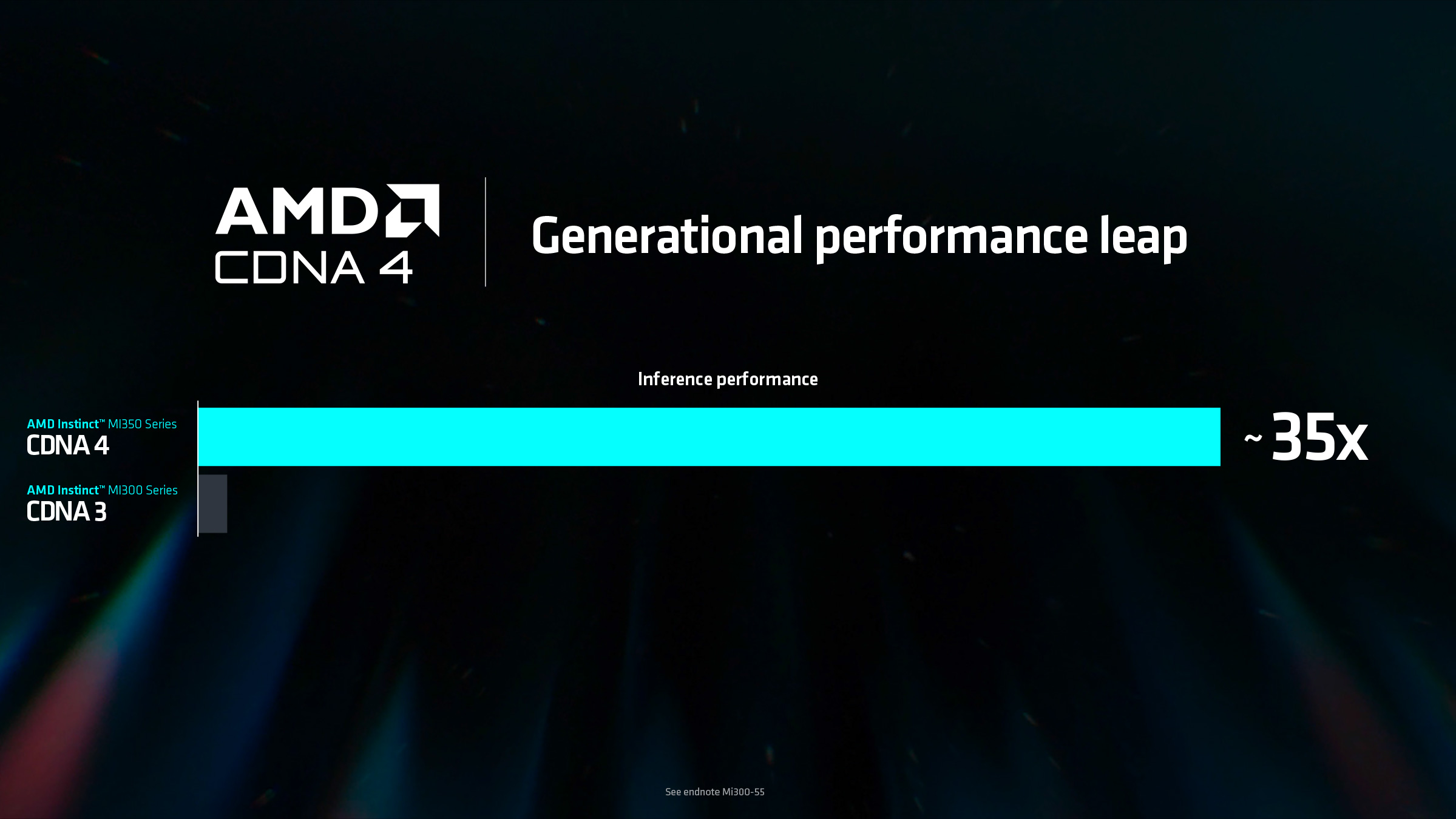
Regarding performance, AMD is touting a 35x improvement in AI inference for the MI350 compared to the MI300X. AMD's footnotes show that this comparison is based on an 8-way MI350 node versus existing 8-way MI300X nodes, using a 1.8 trillion GPT MoE model. This likely takes full advantage of FP4/FP6 support and the larger memory pool, serving as a proxy test for memory/parameter capacity rather than pure FLOPS throughput.
These CDNA 4 compute chiplets will be paired with HBM3E memory, similar to the MI325X. While AMD has not announced specific memory clock speeds, they have confirmed that MI350 accelerators will feature up to 288GB of memory, suggesting using eight memory stacks in top-end CDNA 4 accelerators.
CDNA 4 will be a straightforward upgrade from CDNA 3, adding FP4/FP6 support without drastically altering the compute architecture. AMD’s decision to continue branding it under the MI300-series rather than moving to MI400 indicates a deliberate choice, contrasting with their tendency to iterate product numbers more rapidly in other segments.
Following CDNA 4 in 2025, AMD plans to introduce the CDNA "Next" architecture in 2026, which will power the MI400 series of accelerators. While details are scarce, AMD has emphasized that this will be a "significant" architectural upgrade over CDNA 4. This suggests major changes to the core computing architecture, marking a notable development as CDNA 3 (presumably CDNA 4) can trace its ISA roots back to the 2017 GCN 5 (Vega) architecture.
Overall, AMD is committing to an annual CDNA roadmap cadence starting in 2024, shifting from the previous 2-year cadence. This accelerated product schedule reflects AMD’s rising fortunes and rapid growth in the accelerator industry. However, it remains to be seen how well they can sustain this pace, given the high costs of developing cutting-edge chips. With rival NVIDIA making a similar announcement just 24 hours earlier, the race in the accelerator industry is accelerating.
Subscribe to my newsletter
Read articles from Spheron Network directly inside your inbox. Subscribe to the newsletter, and don't miss out.
Written by

Spheron Network
Spheron Network
On-demand DePIN for GPU Compute
