ARM Architecture and Instruction Sets
 Ahmed Gouda
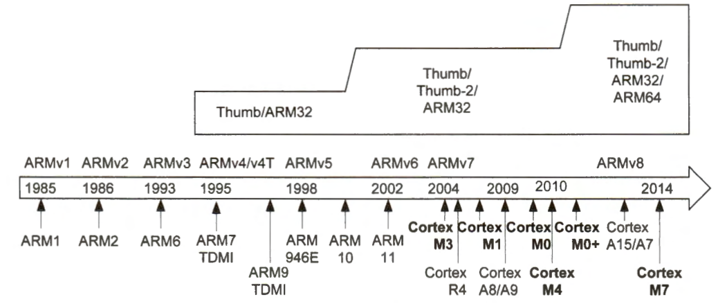
History of ARM Architecture and Instruction Sets

ARM Assembly Instruction Sets
ARM processors support mainly four different assembly instruction sets:
Thumb
Thumb-2
ARM32
ARM64
Thumb
The objective of the Thumb instruction set is to improve the code density. Because an instruction in Thumb has only 16 bits in length, the size of their executable files is small. The space saving is achieved by reducing the possibilities of operands and limiting the number of registers that are accessible by an instruction. Reducing the size of instruction memory benefits many embedded systems demanding for low cost and long battery life.
Code density is a measure of how much functionality can be packed into a given amount of memory space. It is often expressed as the number of bytes required to encode a given set of instructions. Higher code density means that more functionality can fit into a smaller memory area.
ARM32
Each instruction in ARM32 has 32 bits and provides more coding flexibility than a Thumb instruction. More operand options, more flexible memory addressing schemes, larger immediate numbers, and more addressable registers can be encoded in a 32-bit word. Furthermore, ARM32 instructions run faster than Thumb because an instruction can perform more operations or include more operands. However, the disadvantage is its code density.
Thumb-2
It provides an outstanding compromise between ARM32 and Thumb. It optimizes the tradeoff between code density and processor performance. It consists of 16-bit Thumb instructions and a subset of 32-bit ARM32 instructions. The goal of Thumb-2 is to achieve higher code density like Thumb and fast performance comparable to ARM32.
ARM64
ARM 64-bit processors are often used in desktops and servers. These processors have a set of 64-bit assembly instructions.
ARM Cortex Family
One prominent ARM family is Cortex processors, which have three groups:
Cortex-M series for microcontrollers (M stands for microcontroller)
Cortex-R series for real-time embedded systems (R stands for real-time)
Cortex-A series for high-performance applications (A stands for application)
ARM Cortex-A
Cortex-A processors are specially designed based on the ARMv7-A or ARMv8-A architecture to provide fast performance for sophisticated devices, such as smartphones and tablets. They often support full-fledged operating systems such as Linux, iOS, and Android.
ARM Cortex-R
Processors are designed for mission-critical real-time systems that require high reliability, fault-tolerance, and most importantly, deterministic real-time responsiveness. Example systems include factory automation and automobile engine control. In real-time systems, the correctness of computation is determined not only by the logical correctness but also by whether it is consistently completed within certain time constraints.
ARM Cortex-M
processors offer an excellent tradeoff between performance, cost, and energy efficiency. Therefore, they are suitable for a broad range of microcontroller applications, such as home appliances, robotics, industrial control, smart watch, and internet-of-things (IoT). In contrast to general-purpose processors in desktops, a microcontroller is a small processor with a processor core, memory, and many integrated I/0 peripherals such as timers, analog-to-digital converter, serial communications, and LCD driver.
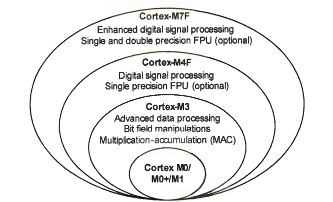
The Cortex-M family includes Cortex-M0, Cortex-M0+, Cortex-M1, Cortex-M3, CortexM4, and Cortex-M7. The former three are Von Neumann architecture, and the latter three are Harvard architecture. Moreover, Cortex-M0/M0+/M1 are ARMv6-M, and CortexM3/M4/M7 are ARMv7-M.

Cortex-M processors are backward compatible. For example, a binary program compiled for CortexM3 can run on Cortex-M4 without any modification.
The floating-point unit (FPU), which is a coprocessor for floating-point operations, is optional on Cortex-M4 and Cortex-M7. Cortex-M4 and M7 also provide single-instruction multiple-data (SIMD) and multiply-and-accumulate (MAC) instructions for digital signal processing applications (DSP).
ARMv7-M only supports the Thumb-2 instruction set and is not compatible with ARM32. Conventional ARM processors are required to switch to the Thumb state to execute a 16-bit instruction and to the ARM state to run a 32-bit instruction. Cortex-M processors can run a mix of 16-bit and 32-bit Thumb-2 instructions without changing the processor state, thus eliminating the overhead of state switching.
Thumb-2 optimizes the tradeoff between code density and application speed.
ARM Cortex-M Architecture
An ARM Cortex-M processor chip consists of:
Cortex-M core licensed by ARM
on-chip peripheral devices implemented by chip manufacturers
buses and bridges for the communication between the core and peripheral devices
Examples of peripheral devices integrated into a Cortex-M chip are LCD controllers, serial communication (I2C, SPI, and USART), USB, digital-to-analog converters (DAC), and analog-to-digital converters (ADC). Different manufacturers may add various peripheral devices to the chip.
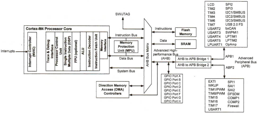
The below figure the core and peripheral devices integrated into the STM32L4 CortexM4 processor chip.

The core processor communicates with the flash memory (typically used as instruction memory), SRAM (generally used as data memory), Direct Memory Access (DMA) controller, and general-purpose input/output (GPIO) ports via a bus matrix (also called crossbar switch).
The bus matrix is an interconnection scheme, which allows concurrent data streams between components connected to the bus matrix, thus providing a high communication bandwidth. The bus matrix connects high-speed components, such as the processor core, Flash, SRAM, DMA controllers, and GPIO ports.
Peripheral devices are connected to the bus matrix via the bus bridges that links the advanced high-performance bus (AHB) and the advanced peripheral bus (APB). Generally, AHB is for high-bandwidth communication, and APB is for low-bandwidth communication. AHB and APB are connected via bridges, which buffers data and control signals to fill the bandwidth gap between these two buses and ensure that there is no data loss.
Each GPIO pin has multiple functions usually. Software can change its function, even at runtime. We can use a pin simply for digital input or digital output, or we can use it for more advanced functions such as analog-to-digital conversion (ADC), serial communication, timer functions, and so on. Different SoC chips may have different GPIO functions, depending on the chip manufacturers.
Most peripheral components, such as timers, ADC and I2C, are connected to APB.
A bus is a set of physical wires for transferring data or control signals between two or more hardware components. A communication protocol or agreement must be in place to coordinate the use of a bus. The bandwidth of a bus depends on the width of the bus (usually specified in bits) and the clock speed supported. A processor has various buses for communicating internal and external hardware components. A bus bridge connects two different buses together.
Fundamental components of a Cortex-M processor core include the arithmetic logic unit (ALU), the processor control unit, the interrupt controller (NVIC), the instruction fetching and decoding unit, and the interfaces for memory and debug.
ALU carries out logical (such as logic AND), and integer arithmetic operations (such as add). ALU has two data inputs (called operands) and one data output.
The processor control unit generates control signals for internal digital circuits (such as the selection signal of the multiplexers, the control signals of the ALU) and coordinates all components of the processor core.
The interrupt controller (NVIC) allows the processor core to stop the execution of the current task and immediately respond to special events or signals generated by software or by peripheral devices.
The instruction fetching and decoding unit reads one machine instruction from the instruction memory address pointed by the program counter and decodes the instruction to figure out what operations the processor core should perform. The processor control unit then generates corresponding control signals based on the decoding result.
The memory interface supports the access to memory devices (such as SRAM and flash).
The debug interface allows a programmer to use a host computer to start or stop a software program on a Cortex-M processor, and monitor or modify processor registers, peripheral registers, and memory in real-time.
Cortex-M4 supports digital signal processing (DSP) and can optionally have a single-precision floating processing unit (FPU). Cortex-M0/M0+/M1/M3 has no support to DSP and FPU. Compared with Cortex-M4, the optional FPU on CortexM7 can support both single-precision and double-precision operations.
Subscribe to my newsletter
Read articles from Ahmed Gouda directly inside your inbox. Subscribe to the newsletter, and don't miss out.
Written by

Ahmed Gouda
Ahmed Gouda
Embedded Software Engineer who are interested in Embedded Systems Design, Embedded Software, Electrical Engineering, and Electronics, C\C++ programming, Assembly, Computer Architecture, Microprocessors, Microcontrollers, and Communication Protocols.