Pi-Hub PCB
 Amber Yang
Introduction
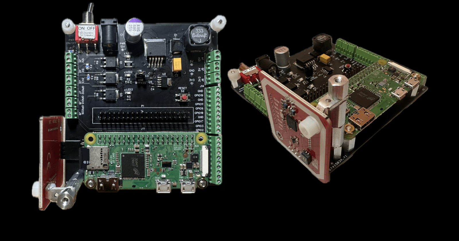
This project is dedicated to the course 'Computer and Electrical Engineering Product Design Project' at Concordia University. The Pi-Hub PCB is designed so that the software team can easily integrate the Raspberry Pi Zero microcontroller with sensors. While we are a team of both software and hardware, only the PCB design is discussed in the blog.
Click here for GitHub repository.
Purpose
The Pi-Hub PCB serves two main purposes:
Power management
Uses wall outlet or battery as the power source
Offers unconditioned 12V, and regulated 5V and 3.3V power outputs
IO expansion
Connectors for sensors
GPIO-enabled MOSFETs
Connector Pinouts
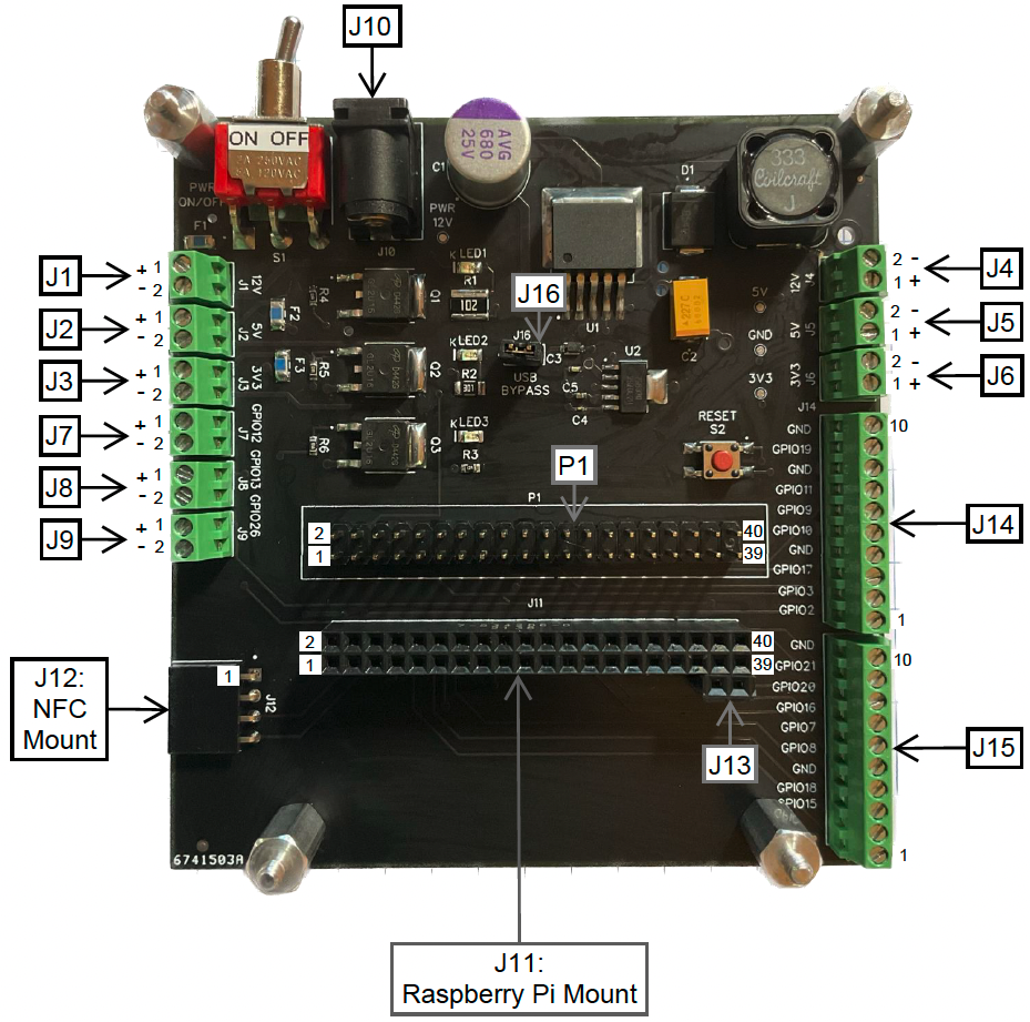
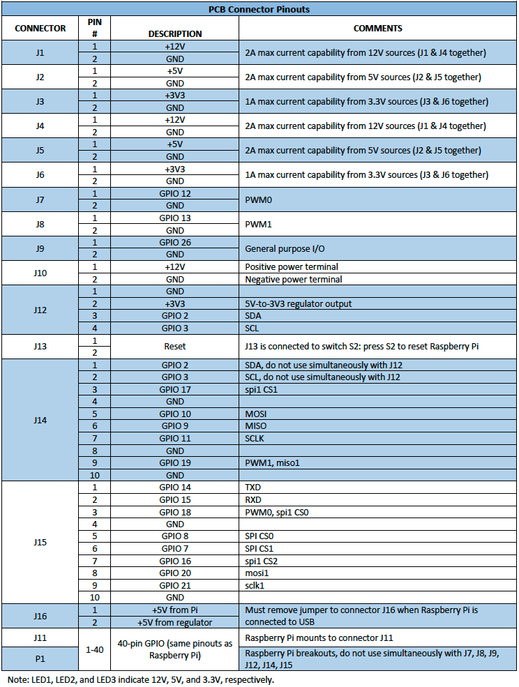
The diagram and table below show the PCB connector pinouts.
Circuit Design & Component Selection
DipTrace EDA is used for schematic capture and PCB layout. This section explains circuit design and considerations, as well as how each component is selected based on design requirements.
12VDC to 5VDC Voltage Regulator
Working Principle
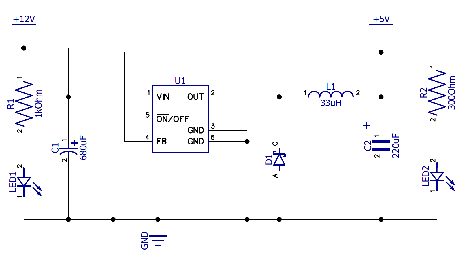
The LM2696 3A step-down switching regulator is responsible for converting 12V to 5V.
It works by rapidly switching on and off, storing energy in an inductor, and then releasing it to the output. This switching action allows it to be more efficient than linear regulators, especially when the difference between input and output voltage is large.
Click here to watch 'Linear and LDO Regulators and Switch Mode Power Supply Tutorial'.
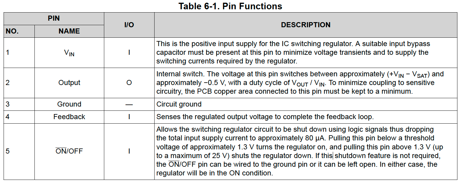
The table below explains each pin's functions:
Linear Regulator VS Switching Regulator Efficiency
Linear regulator maintains a stable output voltage by dissipating excess voltage as heat. The efficiency is given by the formula below:
$$η=\frac{V_{OUT}}{V_{IN}}\times100=\frac{V_{OUT}\times I_{LOAD}}{V_{IN}\times (I_{LOAD}+I_Q)}\times 100$$
We can see that the higher the difference between input and output voltage, the lower the efficiency.
(Quiescent current I_Q is the amount of current the device draws when it is powered on but does not deliver any load current to the output. That is, the regulator's consumption)
Unlike the linear regulator, the average input current of the switching regulator is not the same as the load current due to non-continuous current flow from switching. The efficiency is given by the formula below:
$$η=\frac{V_{OUT}}{V_{IN}}\times100=\frac{V_{OUT}\times I_{LOAD}}{V_{IN}\times (I_{IN}+I_Q)}\times 100$$
For our PCB, we choose a switching regulator to convert 12V to 5V, and a linear regulator to convert 5V to 3.3V. These are the most common operating voltages required for electronic components.
Electrical Characteristics

We can see that this regulator offers 80% efficiency, meaning 80% of the power drawn from the input is delivered to the load (output), while the remaining 20% is lost as heat or other forms of loss within the converter.
The schematic is built following the typical application specified in the datasheet below:

Input Capacitor
The input capacitor is chosen based on guidelines specified in Section 9.1.1 of the regulator's datasheet.


We choose the aluminum polymer capacitor (P/N: 687AVG025MGBJ) with the characteristics to fit the guideline:
Capacitance: 680 µF
- Based on 'Typical Application'
Voltage Rating: 25 V
Input voltage: 12 V
Voltage rating > 1.25 x Input voltage
Maximum RMS Ripple Current: 4.7 A (at 100 kHz, 105°C)
DC load current:
From Raspberry Pi documentation here, Pi Zero typical bare-board active current consumption is: 350 mA
Estimated external current consumption: 4 A
Total DC load current: 4.35 A
Ripple current rating > 50~75% of DC load current
ESR: 0.29256 Ω at 100 kHz
- Equivalent series resistance is low to minimize power dissipation
Note: Polymer capacitors typically have lower equivalent series resistance (ESR) and lower leakage currents than traditional electrolytic capacitors. They also tend to have a longer lifespan and better thermal stability and are often used in high-frequency applications.
Output Capacitor and Inductor
Section 9.1.3 of the regulator's datasheet explains the important parameters for the output capacitor:

The output capacitor and inductor is selected based on the table below:
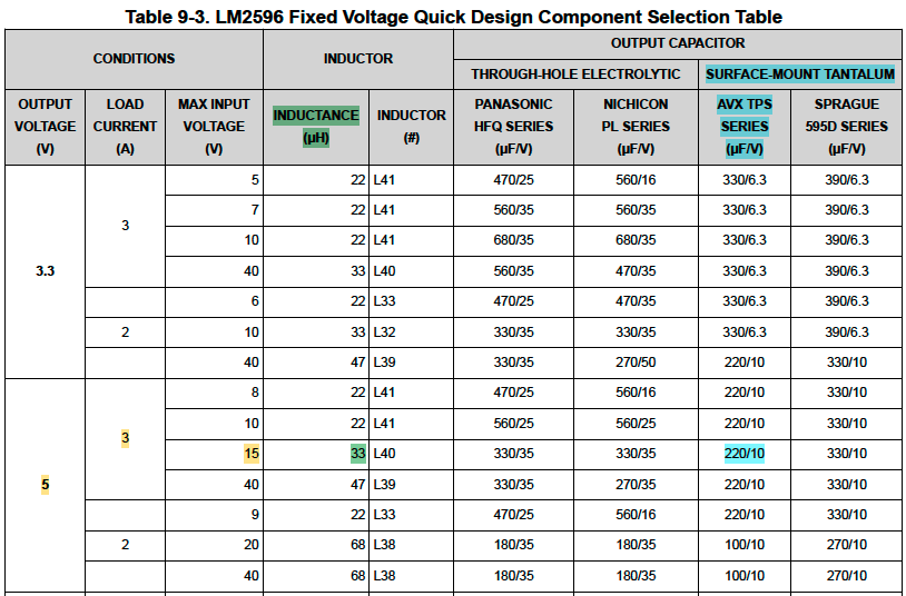
We can see that for a 5V output voltage, 3A load current, and 15V max input voltage, we should choose an inductor of 33uH and a capacitor of 220uF with a minimum 10V voltage rating.
Tantalum ultra low ESR capacitor (P/N: TPME227K016R0025) is selected with the following characteristics:
Capacitance: 220 uF
Voltage rating: 16 V
ESR: 0.025 ohm
The shielded power inductor (P/N: MSS1210-333MED) is selected with the following characteristics:
Inductance: 33 uH
Max DC current: 3.8 A
Catch Diode
The catch diode provides a return path for the inductor when the switch turns off inside the buck regulator.
The diode is selected based on the table below:
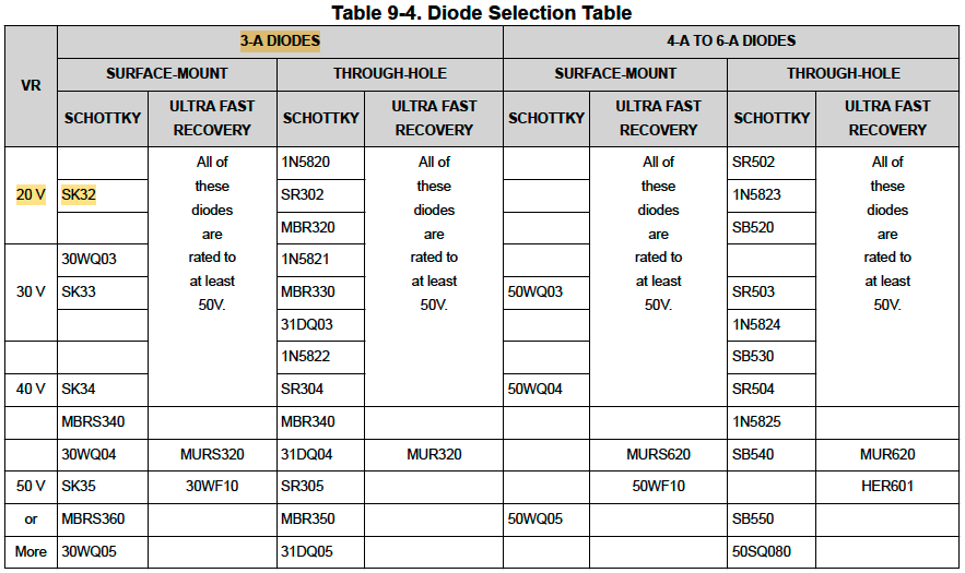
We can see that P/N: SK32 fits the guideline for the 20V voltage rating and 3A current rating. Because we want to supply around 2A current from the regulator, we would like a higher current rating to be safe, the 5A Schottky barrier rectifier (P/N: B540C-13-F) with a 40V voltage rating is therefore selected.
LED and Resistor
The LEDs indicate the 12V, 5V, and 3.3V output voltages are properly operating.
The selected LEDs (P/N: LSM0805452V) have a forward voltage of 2V and a forward current of 20mA. We need to calculate the resistance value and power rating for the resistors. Calculation is shown for 5V supply voltage below:
We reduce the forward current to half to reduce the brightness of the LED and current consumption.
$$Resistance = \frac{Supply\ Voltage - Forward\ Voltage}{Forward\ Current \times 50\%}$$
$$\frac{5V-2V}{0.02A\times50\%} = 300Ω$$
The power rating we choose for the resistor should be at least 5 times the actual power dissipation through the resistor.
$$P=I^2R=(0.01A)^2\times(300Ω)= 0.03W$$
So the power rating for the 300Ω resistor should be at least 0.15W.
The table below shows the resistance value and power rating to put in series with the LED at each voltage output.

5VDC to 3.3VDC Voltage Regulator
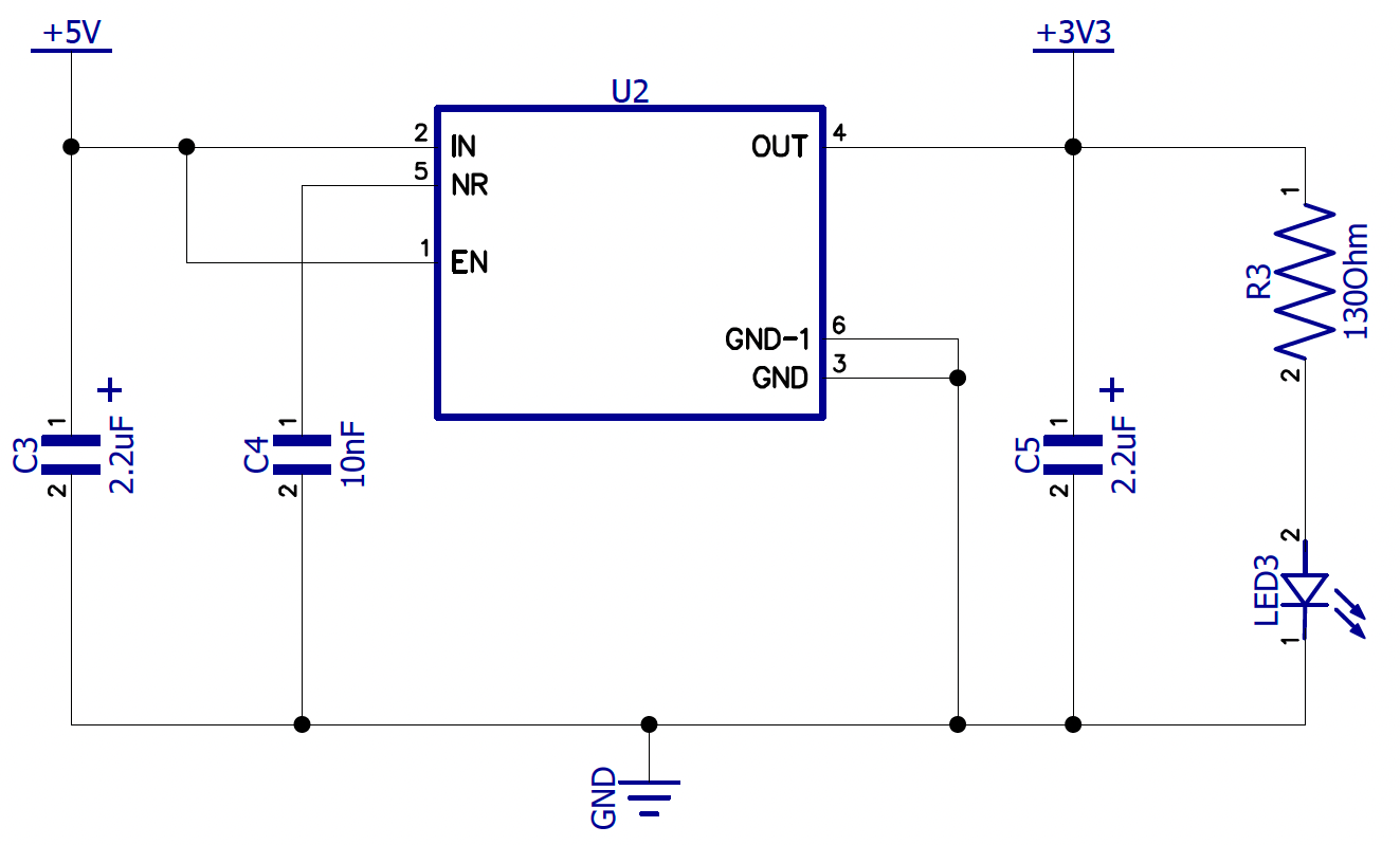
Working principle
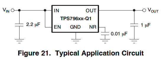
We use the low-dropout linear regulator (P/N: TPS79633) with the following characteristics:
Max input voltage: 5.5V
Fixed output voltage: 3.3V
Output current: 1A
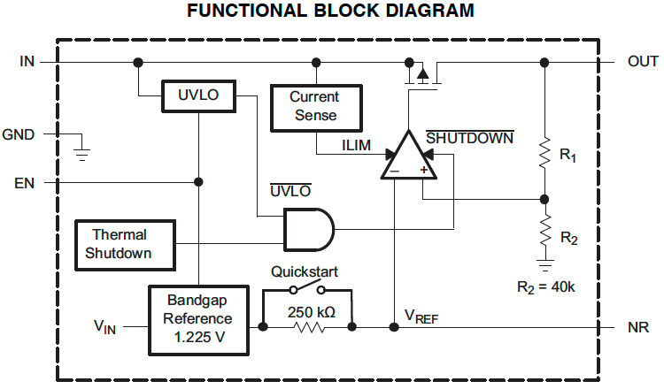
The circuit is built upon the 'Typical Application Circuit' recommended in the regulator’s datasheet below:

External Capacitors
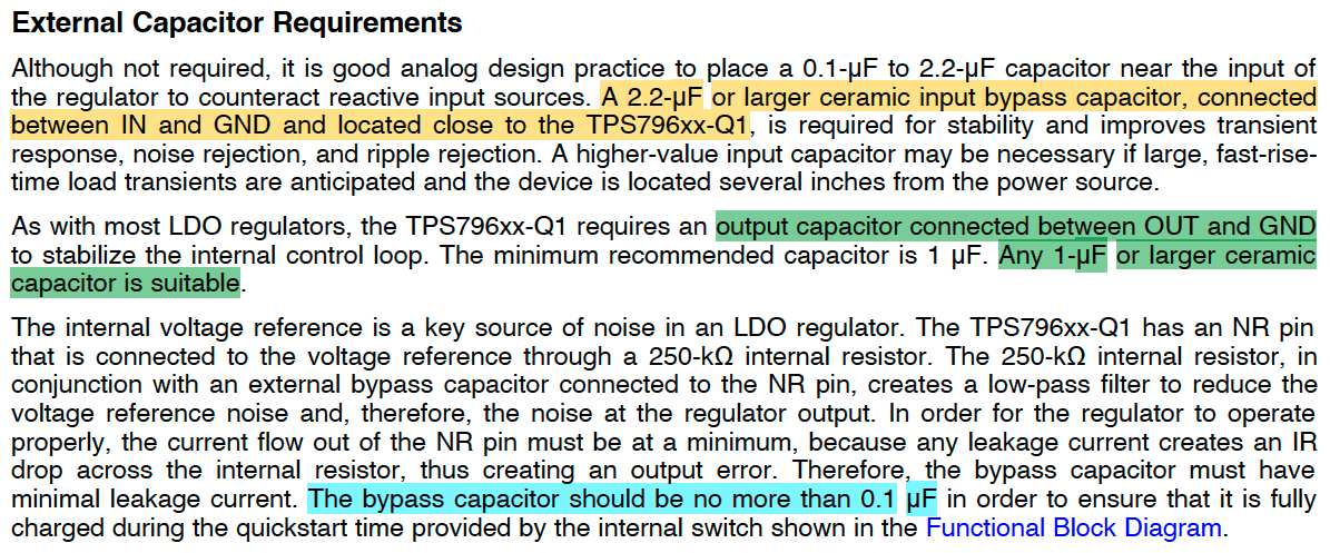
The three external capacitors are chosen based on the requirements specified in the regulator's datasheet:
Power ON/OFF and Power Select
Working Principle
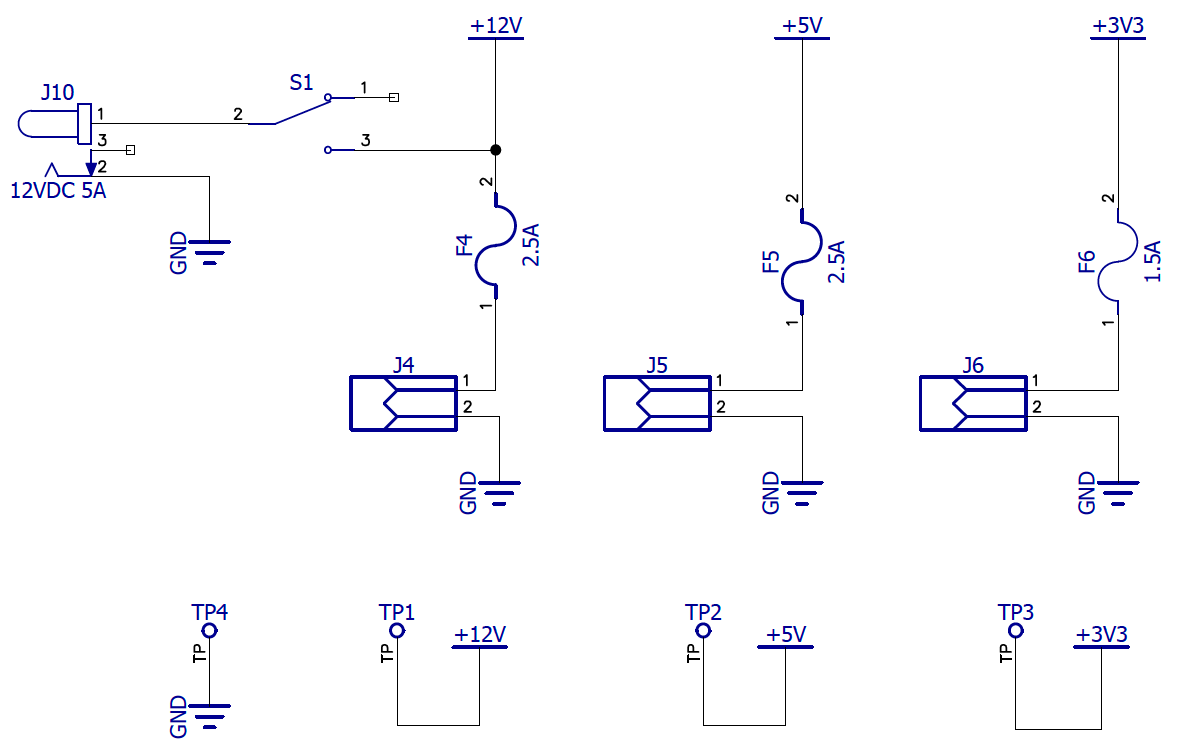
To offer users the flexibility of different output voltages to supply to their sensors, three connectors providing 12V, 5V, and 3.3V are present.
DC power jack (P/N: DCJ200-10-A-K1-K) with 20VDC voltage rating and 5A current rating is used to supply the board with a maximum 5A current. The fuses are present to protect over-current consumption.
GPIO-Enabled MOSFET Switch
Working Principle
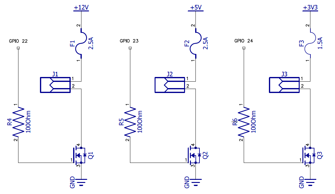
In the case where users do not wish to use constant power from connectors J4, J5, and J6, then connectors J1, J2, and J3 offer the option to use GPIO-enabled outputs to drive higher current devices at different voltage levels.
Note: since the current capability has been increased to 5A in Rev B, the new design now provides 2A max current capability from the 5V sources (J2 & J5 together), and 1A max current capability from the 3.3V sources (J3 & J6 together). The fuses should be updated in Rev B to handle such current loads.
MOSFETs are used as switches by using a control voltage V_GS applied to the gate terminal. When this voltage exceeds the threshold, it forms a conductive channel between the drain and source, allowing current to flow (switch on). On the other hand, when the gate voltage is below the threshold, the switch is off.
Click here to watch 'MOSFETs and How to Use Them'.
Electrical Characteristics
We choose the MOSFET (P/N: AOD442G) with the following characteristics:
V_DS (Drain-Source Voltage):
Max voltage the MOSFET can handle between the drain and source
60V
I_D (Continuous Drain Current):
Max continuous current the MOSFET can pass when fully turned on.
40A at V_GS = 10V
R_DS(on) (On-Resistance):
Low on-resistance means less power losses
Less than 23mΩ at V_GS = 4.5V
V_GS(th) (Gate Threshold Voltage):
The voltage required at the gate to start turning the MOSFET on
1.5V to 2.7V
R_θJA (Thermal Resistance, Junction to Ambient):
How effectively the MOSFET can dissipate heat to the air without heatsinks
40 ~ 50°C/W
T_J (Junction and Storage Temperature Range)
Temperature limits for the MOSFET to safely operate
-55 ~ 150°C
Thermal Consideration
To know if a heatsink is needed for the MOSFET, we need to calculate:
- Power dissipation of the load:
$$P_{LOAD} = I_{LOAD}^2\times R_{DS(ON)} = (2A)^2\times 23mΩ = 92mW$$
- Max power dissipation the MOSFET can handle without a heatsink
$$P_{MAX} = \frac{T_{J(MAX)} - T_A}{R_{θJA}} = \frac{150°C -25°C}{50°C/W} = 2.5W$$
We can see that a heat sink is not needed for our application.
Raspberry Pi IO Expansion
Working Principle
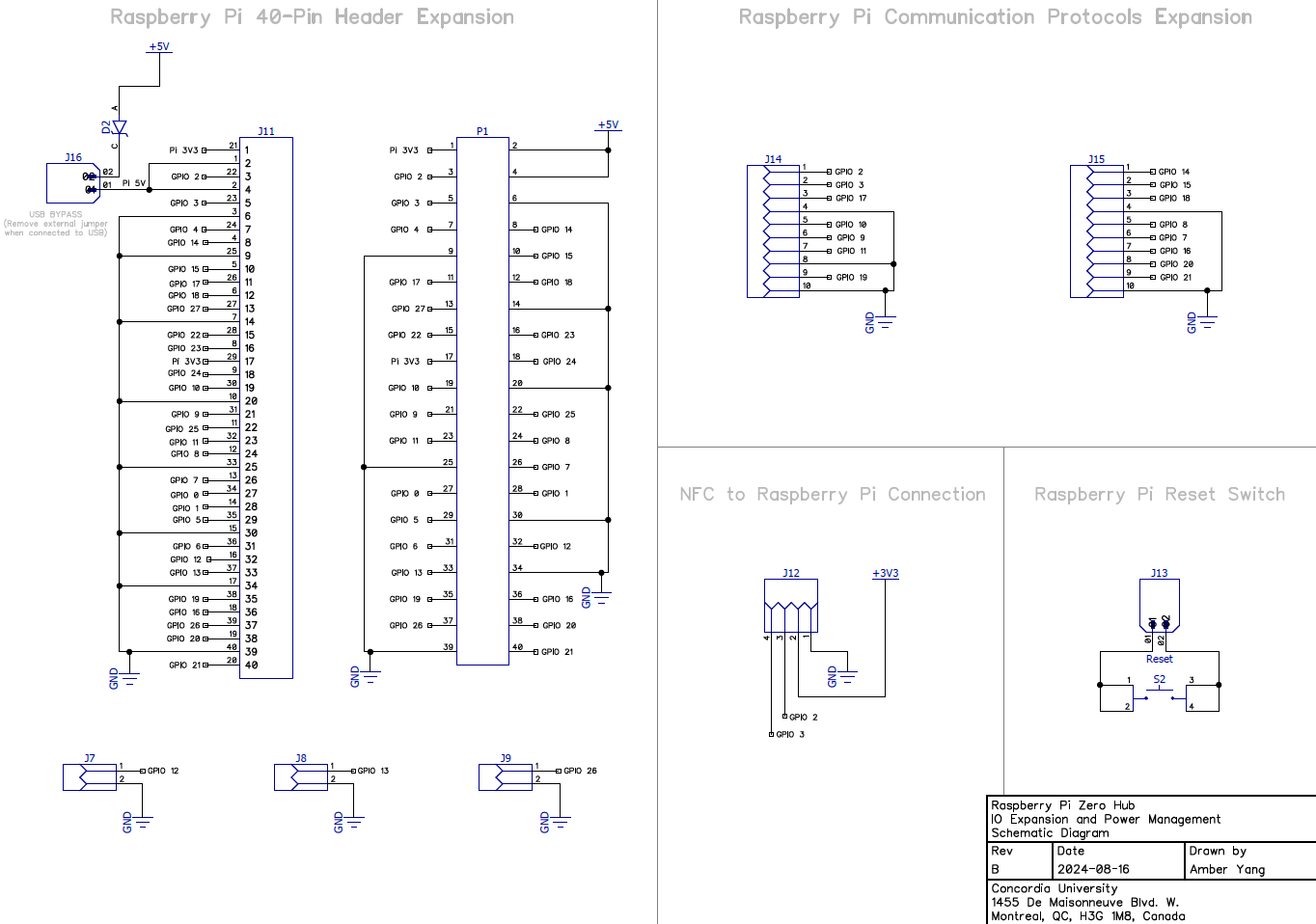
The purpose of this I/O expansion circuit is to extend the number of GPIO (General Purpose Input/Output) pins and communication interfaces available for various peripherals and sensors. This facilitates prototyping and offers flexibility for the users.
During the software development phase, we may connect the Raspberry Pi to a PC. In this case, the PC can supply 5V to the board, and the USB bypass jumper at J16 needs to be removed to make sure no clashing of power sources. A diode is present to prevent back drive in the event the jumper is not removed.
Schottky diode (P/N: CUS08F30,H3F) is chosen for its low forward voltage because we want to supply 5V to power the Raspberry Pi. It has the following characteristics:
Reverse voltage: 30V
Average rectified current: 800mA
Forward voltage: 0.4 ~ 0.45V at 800mA
PCB Layout & Considerations
This section explains the considerations taken into account when doing the PCB layout. This PCB consists of 4 layers:
Top layer
Power plane (12V, 5V, 3.3V)
Ground plane
Bottom layer
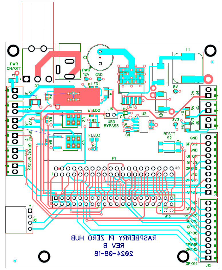
The figure below is an overview of the layout showing only top and bottom layers.
Click here to access the Gerber file.
Component Placement
Power Path
- Place power components like capacitors, inductors, and voltage regulators (e.g., C1, C2, U1, L1) as close as possible to the power inputs and the respective ICs to minimize power losses and noise.
Proximity:
- Place decoupling capacitors (like C3-C5) as close as possible to the power pins of ICs and other sensitive components to filter out noise and provide stable power.
Grounding:
- Ensure good grounding practices by placing ground connections (GND) close to components that generate noise, such as switching regulators or oscillators, to create a solid ground plane.
Logical Flow:
- Position components based on the signal flow in the circuit. For example, keep connectors (e.g., J7-J16), resistors, and transistors (Q1-Q3) near their associated signal paths.
Power and Ground Planes
Dedicated Planes:
- Use separate layers for power (e.g., +12V, +5V, +3.3V) and ground (GND) to minimize interference and improve signal integrity.
Thermal Management:
Ensure that power planes are wide enough to handle the expected current and prevent overheating, especially around components like regulators and high-current paths.
For components like voltage regulators (U1, U2), ensure there is sufficient thermal relief and, if necessary, use vias to connect to a larger copper area to dissipate heat.
Test Points:
- Include test points (e.g., TP1-TP4) for critical signals and power lines to facilitate debugging and validation during testing.
Signal Integrity
Trace Width:
- Make sure the traces for high-current paths are wide enough to handle the current without excessive heating or voltage drops (e.g., power lines feeding the Raspberry Pi header).
Signal Traces:
- Keep signal traces short and direct, particularly for high-frequency signals like clocks or communication lines (e.g., GPIO connections on J1-J16).
Minimize Crosstalk:
- Keep sensitive analog or communication signals (e.g., GPIO or I2C lines) away from noisy power or switching signals.
Avoid 90-Degree Turns:
- Use 45-degree angles for signal traces to reduce impedance discontinuities and signal reflections.
DRC Checks
- Finally, run the design rule check (DRC) function to catch potential errors.
Switching Regulator Layout
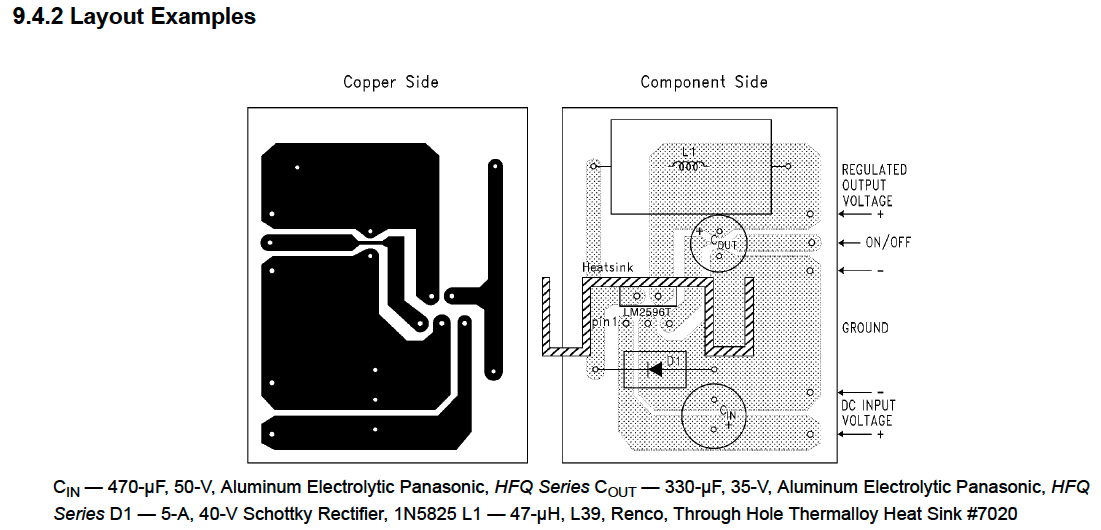
For LM2596 (TO-263 package) switching regulator, we must follow the guidelines in the datasheet to do a proper layout.


Trace Width & Via Diameter
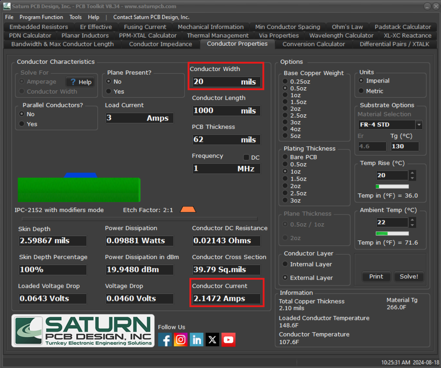
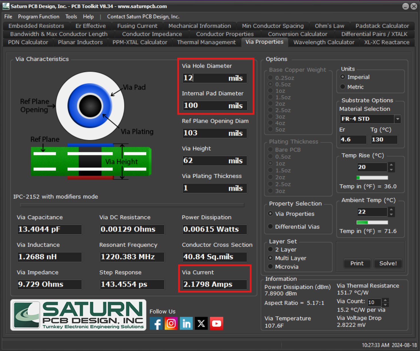
Important parameters such as trace width and via diameter are calculated using the Saturn PCB Toolkit.
For example, to pass 2A current, the conductor width should be at least 20 mils.
Similarly, to pass 2A current through via, the hole diameter should be at least 12 mils and the internal pad diameter should be at least 100 mils.
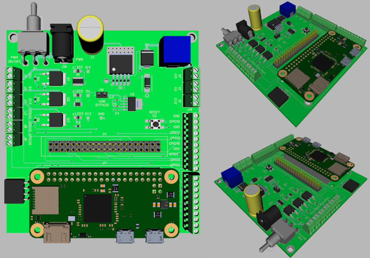
3D Model
The 3D models below help us visualize the components to ensure proper spacing and placement.
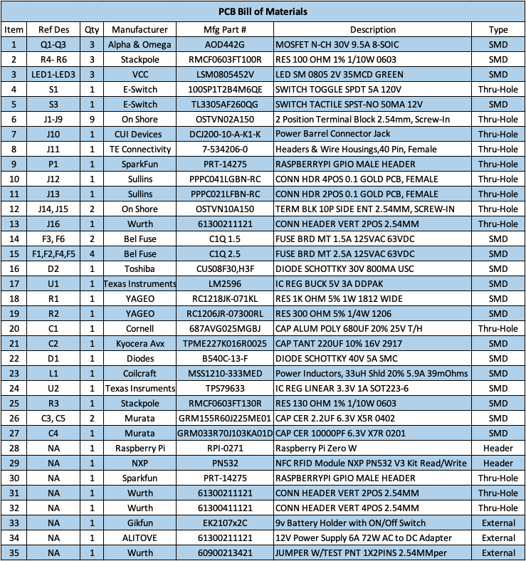
Bill of Materials
The components are purchased from DigiKey and Mouser and the PCB manufacturer is JLCPCB.
Test Cases
The PCB functionality test is designed to detect and confirm the proper functioning of the customized PCB. It validates the PCB and provides stable voltage outputs, correct signal paths, and reliable operation.
The tests are done in parallel with component assembly to ensure each section of the PCB works properly for a successful integration.
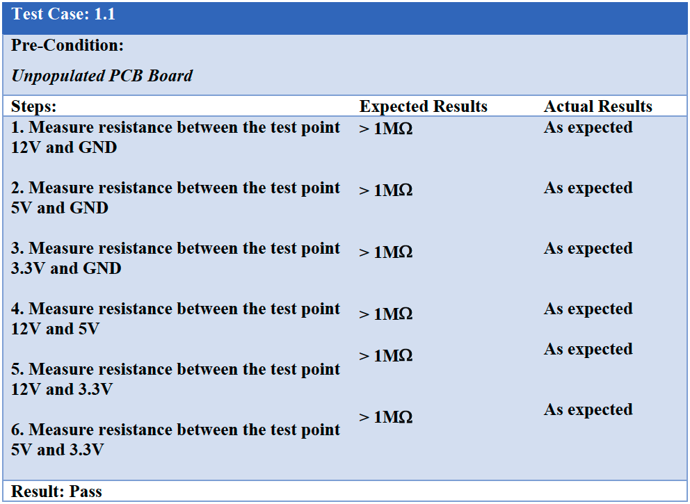
Isolation Check
This test ensures there are no short circuits within the board.
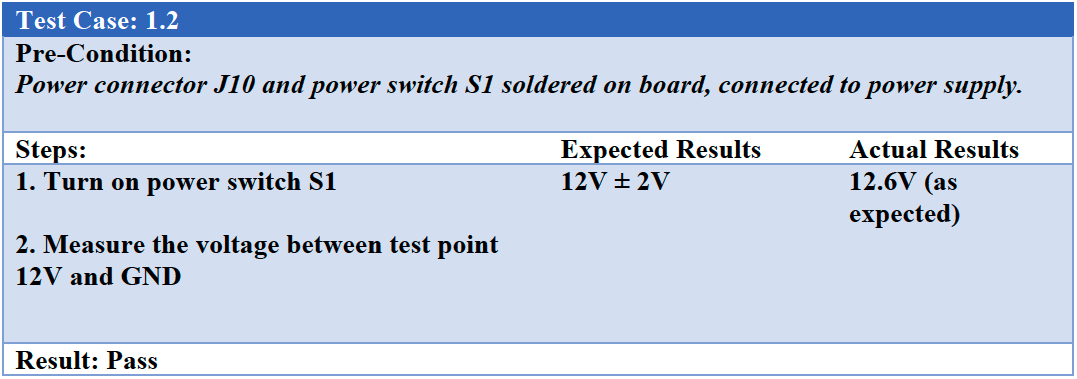
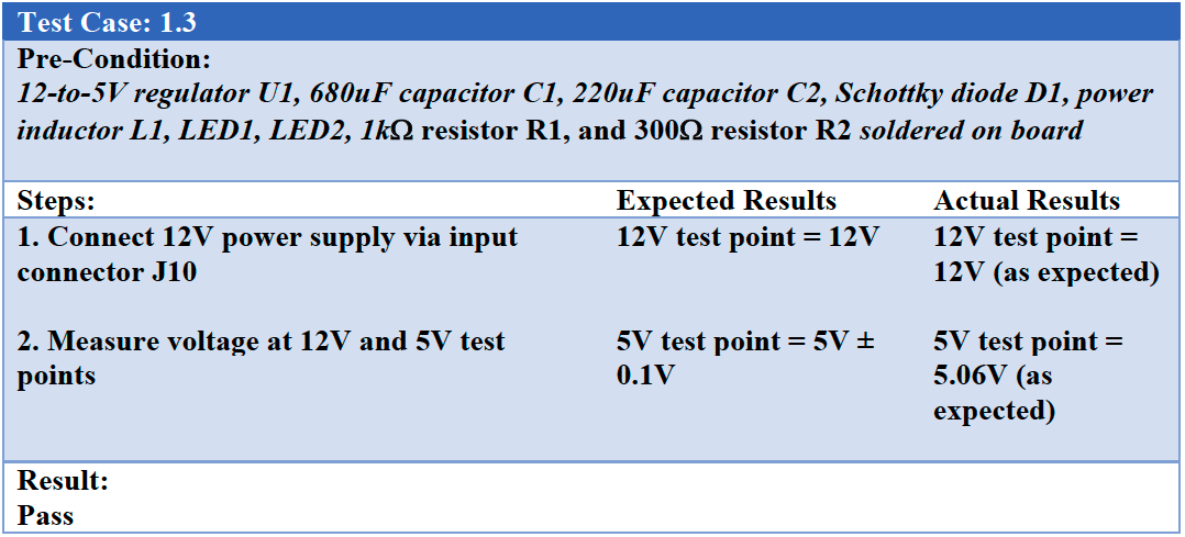
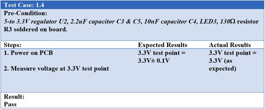
Power Check
This test ensures that the power source and regulators output the correct voltages.
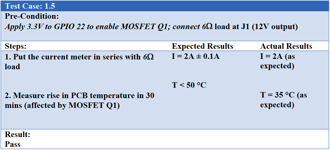
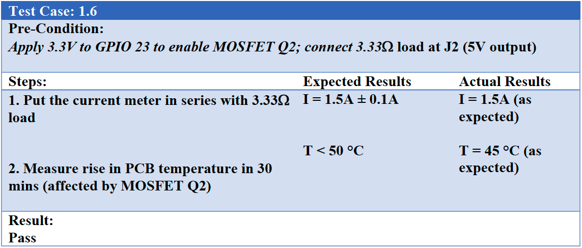
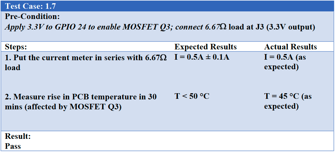
Load Current Check
This test ensures each MOSFET can handle the designated current loads.
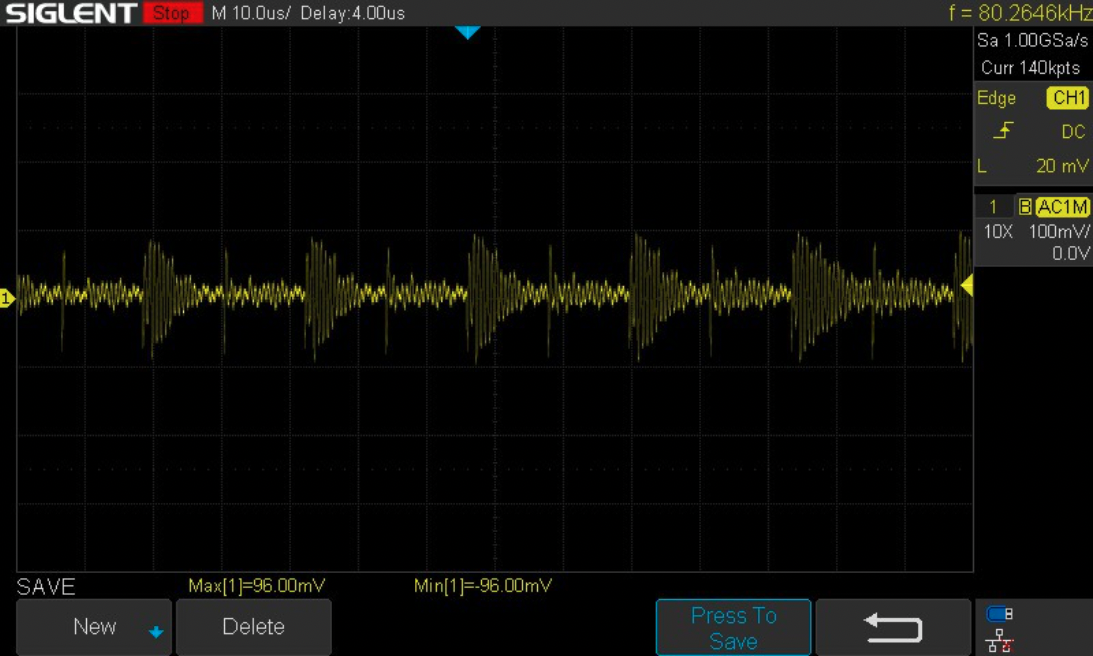
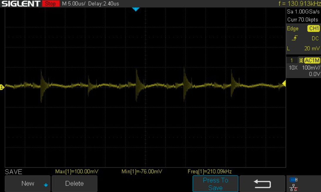
AC Ripples Check
This test ensures the AC ripple at the 5V output stays within acceptable limits under varying loads.
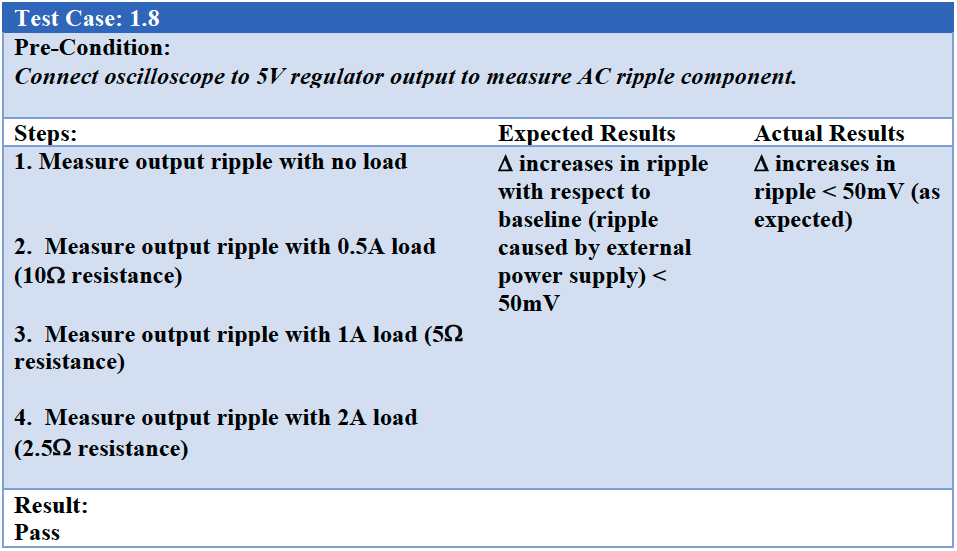
No load:
0.5A load:
1A load:

2A load:

Subscribe to my newsletter
Read articles from Amber Yang directly inside your inbox. Subscribe to the newsletter, and don't miss out.
Written by
