Automation Assembly Compatibility of Double-Sided PCBs
 hitech PCB manufacturer
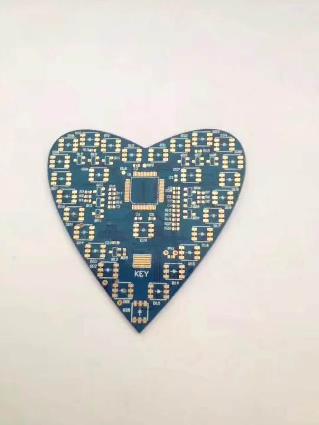
Double-sided PCBs offer increased layout flexibility by allowing components to be placed on both sides. However, automated assembly of double-sided boards presents specific challenges that must be considered during design and production to ensure compatibility with standard manufacturing processes.
- Reflow Soldering for Double-Sided Assembly
In most cases, double-sided boards go through two reflow soldering processes:
First reflow: SMD components are placed on one side and soldered
Second reflow: The board is flipped, and the opposite side is assembled and reflowed again
Considerations:
Components on the first side must withstand a second reflow cycle
Use adhesives to secure heavier components that may fall off during the second reflow
Choose reflow profiles carefully to avoid thermal stress
- Component Placement Strategy
Proper planning of which components go on each side is crucial:
Place heavier or through-hole components on the second side (hand-soldered or wave-soldered)
Place smaller, thermally stable components on the first side for double reflow
Avoid placing high-profile components directly opposite each other to prevent collision during pick-and-place
- Wave Soldering Considerations
When combining SMT and through-hole:
SMT components on the bottom side must be able to withstand wave soldering
Use glue or adhesives to secure bottom-side SMT parts
Ensure component orientations and clearances are wave-solder-compatible
- Fixturing and Support
To protect components during automated processing:
Use custom fixtures or pallets to support the assembled side
Provide component clearance zones to avoid crushing or misalignment
Avoid placing fragile components near the board edges
- Solder Paste Printing
For double-sided reflow:
Solder paste is applied to each side separately
Ensure accurate alignment and stencil thickness to avoid bridging
For very dense designs, consider step-down stencils to balance solder volume
- Inspection and Testing Compatibility
AOI must be set up for both sides
Fixtures for ICT or functional testing should avoid damaging components already placed
Use test points accessible from one side if possible to simplify fixture design
- Design for Manufacturability (DFM) Guidelines
To improve automated assembly success rate:
Group components by size and thermal profile to minimize reflow defects
Use fiducial marks on both sides for alignment
Maintain consistent polarity marking and silkscreen clarity
Include tooling holes and panelization tabs for efficient handling
Summary
Double-sided PCBs are fully compatible with automated assembly when properly designed and planned. Key factors include thermal considerations, component placement strategy, secure mounting of lower-side components, and using appropriate fixturing and inspection methods. By following DFM best practices, manufacturers can achieve high throughput, low defect rates, and stable production quality.
Subscribe to my newsletter
Read articles from hitech PCB manufacturer directly inside your inbox. Subscribe to the newsletter, and don't miss out.
Written by
hitech PCB manufacturer
hitech PCB manufacturer
Hitech – Your one-stop electronics manufacturing service provider and partner in China, we offer rapid PCB boards, PCB assembly, electronic parts and electric appliances for different applications.