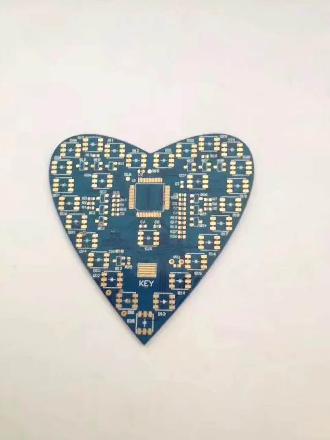
Thermal Management Design for Double-Sided PCBs
 hitech PCB manufacturer
Efficient thermal management is essential for the performance and reliability of double-sided printed circuit boards (PCBs), especially when high-power components or dense assemblies are involved. Improper heat dissipation can lead to solder joint failure, component damage, and reduced product lifespan. Below are key thermal management techniques and design considerations specific to double-sided PCBs.
- Importance of Thermal Management
Prevents overheating of components
Reduces thermal stress on solder joints and PCB materials
Ensures stable performance in high-temperature environments
Increases overall product reliability
- Common Heat Sources in Double-Sided PCBs
Power semiconductors such as MOSFETs and voltage regulators
High-brightness LEDs
Power ICs and processors
Analog and RF amplifiers
- Thermal Management Techniques
3.1 Copper Pour and Thermal Vias
Use large copper planes on both sides of the board to spread heat
Add thermal vias to connect top and bottom copper layers, improving vertical heat flow
Vias should be filled or tented if placed under components
3.2 Heat Sinks
Attach external heat sinks to high-power components
Use through-hole or surface-mount heat sink packages
Ensure good thermal contact using thermal paste or adhesive
3.3 Thermal Pads and Heat Slugs
Many components have thermal pads that must be soldered to copper areas
Use solder mask openings under thermal pads to allow better solder wetting
Incorporate exposed copper slugs in the PCB design for improved heat transfer
3.4 Board Stack-up and Material Selection
Choose PCB substrates with high thermal conductivity, such as FR4 with thermal-enhanced fillers or metal core PCBs
Use thicker copper (e.g., 2 oz instead of 1 oz) for better heat dissipation
Consider using aluminum base or ceramic substrates for extremely high heat loads
3.5 Placement Strategy
Spread high-power components across the board to avoid hot spots
Keep sensitive analog or RF circuits away from heat-generating parts
Place components with thermal pads close to copper pours or via arrays
3.6 Ventilation and Enclosure Design
Ensure the enclosure allows proper airflow around the PCB
Use fans or ventilation slots if natural convection is insufficient
Avoid trapping heat between double-sided assemblies
- Thermal Simulation and Testing
Use thermal analysis software to simulate heat flow and identify critical areas
Measure temperature during operation using thermocouples or infrared cameras
Perform thermal cycling tests to evaluate solder joint fatigue
- Design Tips Summary
Increase copper area and via count for heat-spreading
Connect thermal pads to large copper zones with multiple vias
Choose heat-tolerant components and materials
Ensure PCB layout aligns with mechanical thermal solutions like heat sinks and airflow
Validate design with simulation and real-world testing
Conclusion
Thermal management is a vital part of double-sided PCB design, especially in power electronics, LED lighting, automotive, and industrial systems. By combining smart PCB layout, suitable materials, and mechanical heat-dissipation techniques, designers can effectively manage temperature and ensure long-term product reliability.
Subscribe to my newsletter
Read articles from hitech PCB manufacturer directly inside your inbox. Subscribe to the newsletter, and don't miss out.
Written by

hitech PCB manufacturer
hitech PCB manufacturer
Hitech – Your one-stop electronics manufacturing service provider and partner in China, we offer rapid PCB boards, PCB assembly, electronic parts and electric appliances for different applications.